Customer
The Russian company producing game machines.
Task
To analyze the possibilities of developing a game machine with the resolution of 1600х1200 pixels and the vertical-repetition frequency of 60Hz. The video data shall be generated from four layers by the superposition method on the basis of transparency channel in every layer.
Every image layer is generated from the ready dot-matrix fields of 8х8 pixels, the total amount of dot-matrix fields being 128KB. The dot-matrix fields are stored in the ROM and after the boot they are rebooted to be read subsequently into the faster DDR memory. Dot-matrix field pointers are read from the video RAM independently for every layer.
The current address of the video RAM used for reading a dot-matrix field pointer is generated from the current line number, dot-matrix field number in the line and horizontal and vertical shift data. The current shift data are generated independently for every layer and can be not multiple of 8 pixels, the above data are determined for every layer by the soft-processor and can vary when in use. The shits may be positive and negative.
Solution
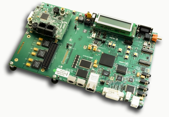
After the preliminary estimate, analysis of the resource requirements and that of the new program modules, as well as the computation of time required for the performance of the problem put by (taking into account the existing program modules and IP-cores), the following goals have been set: to estimate the possibilities of developing a game platform and to perform testing of core modules mounted on the finished board by Xilinx Spartan-3A DSP FPGA Video Kit.
Concept development
There are three main algorithms of video data generation implemented and tested in the project:
- The mode of video data generation with one line caching. In the current mode two buffers of the internal block memory with the whole line length of 2048 symbols and the width of 24 bits (8 bits for each color component R, G and B) have been used. The algorithm is as follows: at the digital active line, while the information is being read from one buffer, another buffer is being filled up with the next generated line. I.e. at the digital active line and the line blanking interval the proofreading of the current dot-matrix field line data at all four layers shall be performed taking into account the shifts, and they shall be mixed and uploaded into the block memory — and so on along the whole line. Taking into consideration that dot-matrix field derivation can be random (i.e. data reading from DDR memory is not linear, memory bank closing requires extra time), the total time of the new line generation appears to be longer than the time required for horizontal line pass at the resolution 1600х1200х60 pixels. As a result this feature limits the application range of the current algorithm.
- The mode of video data generation with eight lines caching, i.e. at the whole dot-matrix field width. Two buffers as well as in the first algorithm are used here: one is read and the other is generated. In the current algorithm all dot-matrix fields are uploaded into DDR memory linearly in one line, this allows to read all dot-matrix fields without bank closing. As a result it considerably reduces the time of the new line generation at the resolution of 1600х1200х60 pixels. However the current mode requires high capacity of internal block memory, in this case — 2 (two buffers) х 8 (eight lines) х 3 (three components RGB) = 48 memory banks. This figure exceeds the quantity of internal memory banks arranged in the EPLD project, and it also limits the current algorithm application range.
- The mode of video data generation with the by-turn opening of DDR memory banks. The concept is as follows: all four DDR memory banks contain identical copies of all dot-matrix fields, and each subsequent proofreading is launched from the next bank, while the current one is automatically closed. Thus by the time the reading of this bank starts again, it will already be in the off condition. Such an approach allows to perform proofreading without interrupting reading at the whole digital active line for the max resolution.
The latter algorithm has been taken as a basis for this project. It considerably saves EPLD internal resources and does not constrain system performance as a whole. It is the disadvantage of this algorithm that it is required to use two stand alone special controllers and large capacity of DDR memory for four layers.
Hardware platform design
XC3SD3400A-4FGG676CES EPLD by Xilinx is the main board.
The following modules and controllers are mounted onto the EPLD:
- CH7301C-TF DVI-I video signal output controller. It has been used for the output of graphic data to the monitor
- DDR2 memory module with the data bus of 32 bits. It has been used for the storage of dot-matrix fields of 8х8 pixels
- ZBT RAM CY7C1354C-166AXC static memory (ZBT — Zero-bus turnaround). It has been used for the storage of dot-matrix field pointers for two layers
- IDT5V9885PFGI programmable clock generator
- Security modules and board supply voltage generators
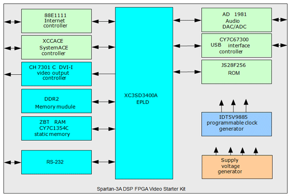
Picture 1. Layout of the structure of XC3SD3400A-4FGG676CES EPLD by Xilinx
Software development
The basic language of modules — VHDL.
During the engineering process the following modules are written and modified:
- DDR memory controller is modified. It allows to perform proofreading of the dot-matrix fields in the real-time at the digital active line.
- Arbiter of DDR controller data is developed to separate write buses from soft-processor and read bus for the layers generation logic.
- The block of partitioning layer data during the proofreading from the memory is developed (taking into account horizontal shifts in each layer).
- Layer mixing module is developed taking into account the transparency channel in each layer.
- DVI-controller is developed for generating control signals for the intrinsic logic and DVI-interface signals.
- ZBT RAM controller is developed, it allows to write and read dot-matrix field addresses for each layer at the digital active line.
- ZBT RAM controller arbiter is made for separating write buses from soft-processor and the read bus for each layer address generation logic.
- The module of each layer address generation is developed taking into account horizontal and vertical shifts in each layer.
- PicoBlaze soft-processor for module operation.
- The program is written in the assembler for PicoBlaze. It allows:
- To generate various sets of dot-matrix fields and to upload them into DDR memory.
- To generate dot-matrix field pointers and upload them into the video RAM.
- To generate data for shifts and set them at the command of the user.
- To process the commands received via RS-232.
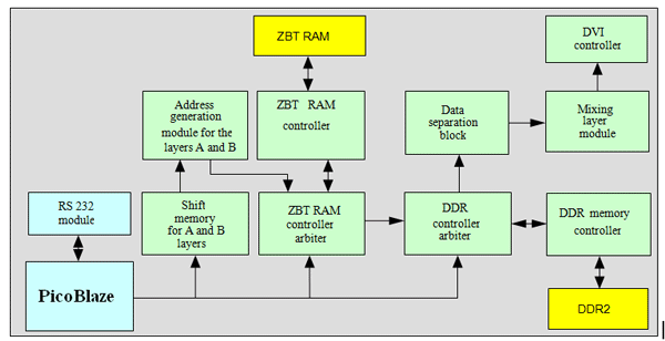
Picture 2. Layout of the structure of the implemented software
Advantages of the designed prototype
- The usage of the ready Spartan-3A DSP FPGA Video Kit board considerably reduced the project implementation time.
- Taking into account the periphery mounted on this board and the recommended restrictions on the system rate, the system performance tests at the whole allowed to considerably reduce restrictions that could appear during the on-site board production.
- As a result of all single and complex module tests performed the complete layout of the functions of the full project implementation is obtained.
Disadvantages of the designed prototype
- The main disadvantage is the insufficient board resources. Namely lacking external DDR memory for the storage of all four layers dot-matrix fields has been detected, that is why only two layers have been used in the project. There is also the lack of resources for the implementation of the 32-bit soft-processor to achieve the full-scale control and interoperation of the whole platform.