
FPGA Projects
SoC and FPGA Design Services
Our team offers FPGA design services, leveraging advanced solutions from world-leading FPGA vendors. Here, we demonstrate our experience via short case studies on Intel, Microchip, Lattice Semiconductor, Xilinx, and NVidia products.
We also specialise in SoC FPGA design services tailored for high-performance applications. SoC FPGAs, combining the flexibility of FPGA with multiple processors on a single chip, enable us to customise hardware acceleration, establish real-time processing, and scale the processing units.
Xilinx ▪ Intel ▪ Lattice Semiconductor ▪ Microchip ▪ NVidia
Xilinx
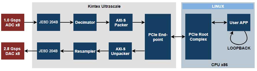
ADC/DAC repeater
Tags: Kintex, Ultrascale, MicroTCA, JESD 204B, Linux, PCIe
We designed firmware for the MicroTCA system for buffering data from ADC in CPU x86 system and translating it to the DAC.– 1 Gsps ADC x8 channels– 2.8 Gsps DAC x8 channels– DMA– PCIe
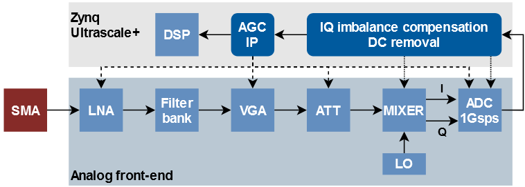
Analog frontend real-time controller
Tags: Zynqus+, SDR, AGC, IQ, AFE
AGC, IQ imbalance compensation, and DC removal algorithms have been implemented in Zynq Ultrascale+. The IP cores and software controls analog frontend board ICs provided parameters in real-time. AGC is table-based. IQ and DC techniques use surrogate optimization algorithm over ADC and mixer tunable parameters.
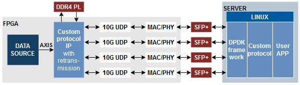
High-speed reliable data transfer over 4x10G
Tags: Zynqus+, Dpdk, 10G, UDP, DDR4
A reliable data transfer chain from FPGA to Server with overall bandwidth up to 38Gbps has been implemented. The DPDK framework used a server-side to allow high-rate data reception. A custom protocol with a retransmission feature has been implemented. The data cached in DDR4 PL external memory.
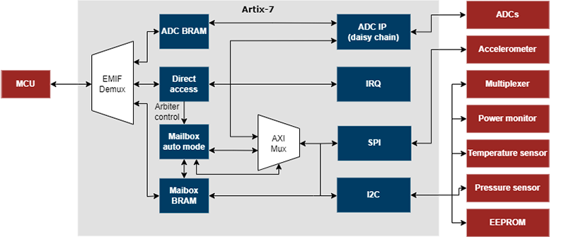
Interface extension FPGA project
Tags: Artix-7, MCU, ADC, SPI, I2C
Interface extension FPGA project.
– big-endian and little-endian support for EMIF
– direct access mode for MCU to end-points
– auto mode for polling end-points in round-robin
– arbiter switch for changing modes of access
– ADC controller with daisy chain support and internal configurable median filter
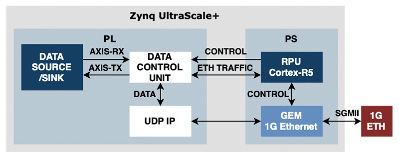
Zynq US+ 1G ethernet
ZynqUS+, Networking, 1G, RPU, Cortex-r5, UDP
An implementation of UDP protocol with hardware Gigabit ethernet controller (GEM). The data can be transmitted both from PL and PS subsystems.
– Hardware UDP offloader
– AXI4-Stream data interfaces
– Control driver for RPU
– Packets routing between PL and PS using IP port
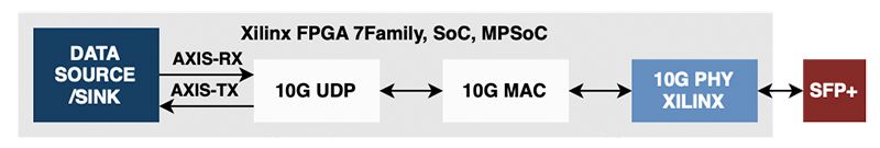
Zynq US+ 10G ethernet
ZynqUS+, Networking, 10G, UDP
A hardware implementation of UDP protocol and 10G MAC.
– Hardware 10G UDP offloader
– AXI4-Stream data interfaces
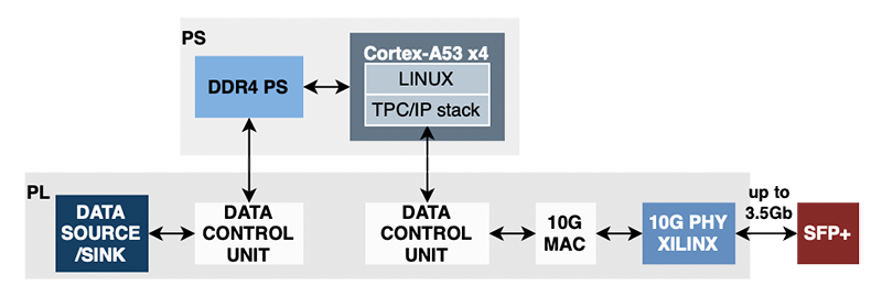
10G TCP/IP using Linux
ZynqUS+, Linux, 10G, TCP/IP, DDR4
The design solves the problem of reliable data transfer from PL to server. Data transferred directly from PS DDR4 via TCP/IP protocol. The achieved bandwidth is 3.5Gb over a 10G interface.
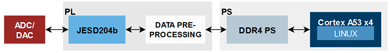
JESD204b data transfer to Linux
ZynqUS+, JESD204b, Llinux, ADC, DAС
A design for high-speed ADC and DAC capturing and streaming from/to PS DDR4 memory. The subsystem runs under Linux application control.
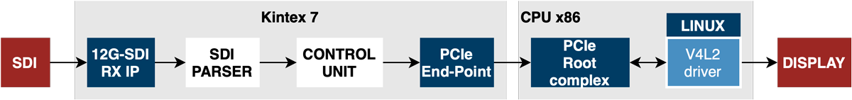
12G-SDI processing
Kintex7, Linux, PCI-E, SDI, Drivers
The design included in the Viewfinder product. Kintex-7 FPGA captures 12G-SDI signal, transmits video data to x86 CPU via PCIe. The Linux receives a video stream using a custom-designed V4L driver and outputs to the display.
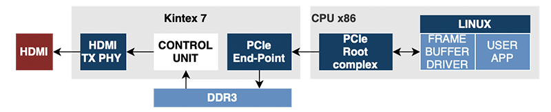
4k HDMI frame buffer
Kintex7, Linux, PCI-E, HDMI, 4K, Drivers
– Linux driver for frame buffer
– Data transfer between x86 CPU and Kintex-7 via PCIe
– DDR3 for image buffering
– Two HDMI output interfaces
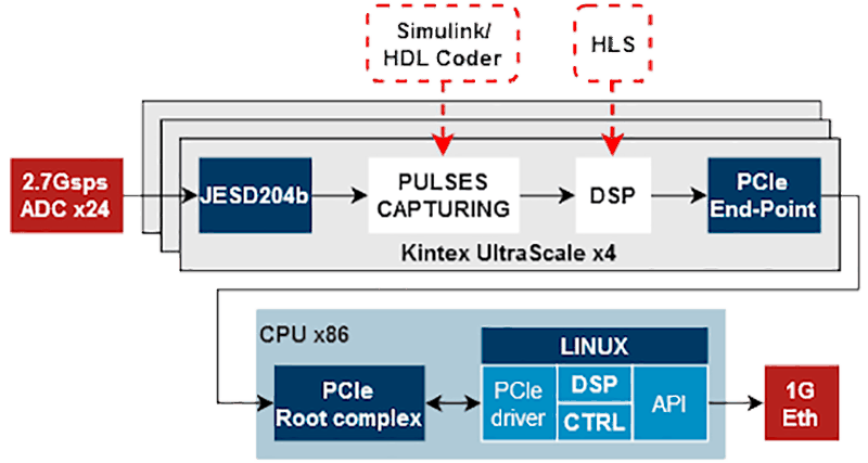
Nano seconds pulses processing
Kintex, Ultrascale+, Linux, MicroTCA, PCI-e, HLS, Simulink, JESD 204b
We designed firmware for the MicroTCA system for the statistical analysis of nanosecond pulses parameters.
– 2.7Gsps ADC x24 channels
– High-level synthesis tools for math
– Data aggregation by Linux
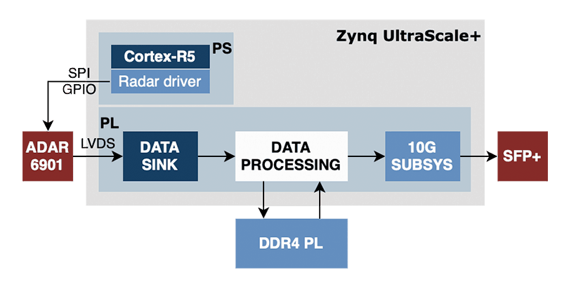
Radar data processing
Zynq Ultrascale+, Cortex-R5, ARM, lvds, 10g
We designed a PCB and firmware for the ADAR6901 radar data processing.
– Zynq UltraScale+
– Cortex-R5 for radar control
– Driver and HAL development
– High-speed LVDS interface
– DDR4 PL for data storage
– 10G interface for processed data downstreaming
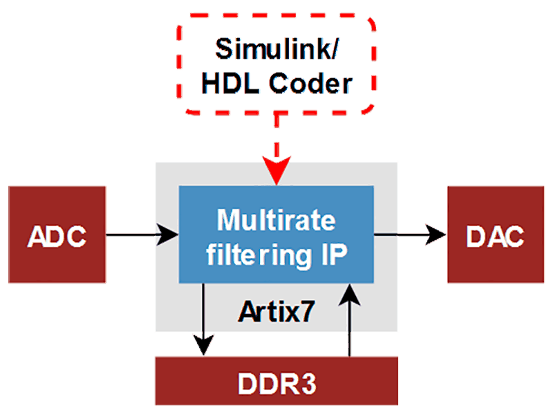
Multirate filter
Xilinx, Simulink, HDLcoder, Artix7
A multirate filter IP core has been generated from the Simulink model using HDL coder toolbox. Signal was buffered in the DDR3 memory for delay implementation.
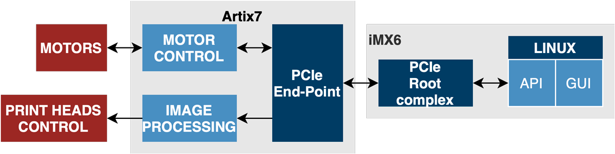
Printer controller
Xilinx, PCIe, Motor, Artix7
Custom solution for industrial printer motor control logic and raster image feeding.
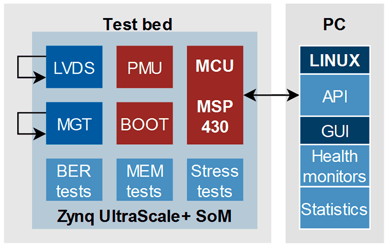
Manufacturing testing equipment
Xilinx, ZynqUS+, MCU, tests
PCB and FW/SW for high-performance ZynqUS+ SoM modules tests at the manufacturing site.
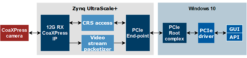
CoaXPress frame grabber firmware
ZynqUS+, CoaXPress
A CoaXPress frame grabber firmware based on PCB hosted Zynq Ultrascale+ MPSoC and Windows 10 machine.
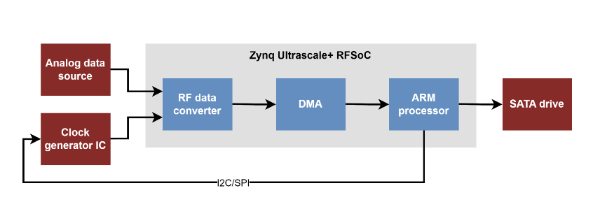
RFSoC ADC data capture
Tags: Zynq US+ RFSoC, ADC, SATA, SDR, I2C, SPI
We developed an ADC data capture system that captures data from 3 ADC channels, transfers them to the PS, and stores them in a SATA drive. The main problem that was solved was to transfer data without gaps from the PL to the PS side. In addition to data capturing, the ARM's software carries out clocking subsystem configuration via I2C/SPI interfaces.
Zynq UltraScale+ RFSoC is a single-chip adaptable radio platform.
Intel
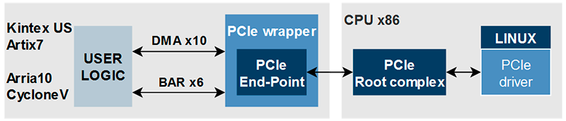
Advanced PCIe End-Point IP core
Kintex, Ultrascale, Artix7, Linux, PCI-e, Intel Arria10, CycloneV
A multiplatform PCIe controller core wrapper providing up to 10 DMA channels and 6 BARs.
– Linux driver
– Kintex UltraScale / Artix7
– Arria10 / CycloneV
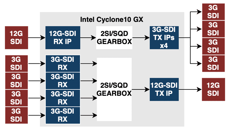
3G/12G SDI gearbox
Intel, Cyclone10, SDI
A complete device has been designed for 3G and 12G signal processing. A custom Gearbox IP core for 4x3G<->12G streams conversion has been delivered with 2SI and SQD modes support.
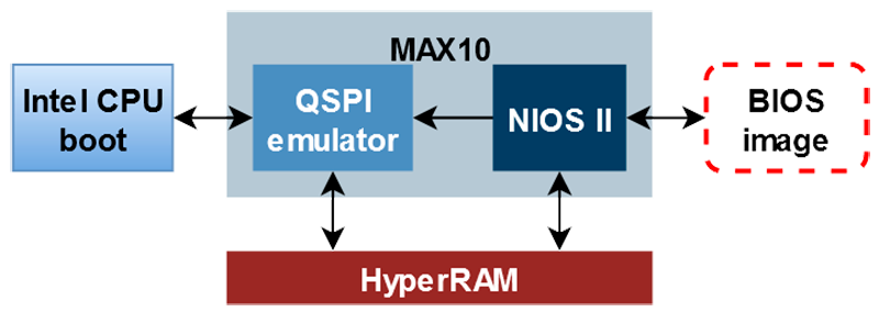
BIOS emulation
Intel, HyperRAM, niosii, max10, qspi
MAX10+HyperRAM based BIOS emulator for secure Intel chipsets booting.
Lattice Semiconductor
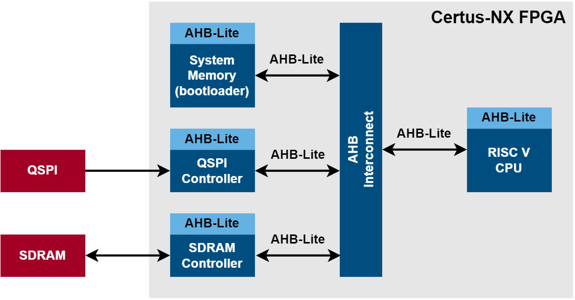
Bootloader Development for the NX FPGA family
Tags: Lattice, RISC-V, bootloader, FPGA, Certus-NX, Сrosslink-NX
Development of a bootloader for the Lattice NX FPGA family with support for external QSPI flash memory. The project included hardware validation on dev boards based on Crosslink-NX and Сertus-NX. The SDRAM IP core can be adapted to the NX architecture and used with the RISC-V synthesizable core.
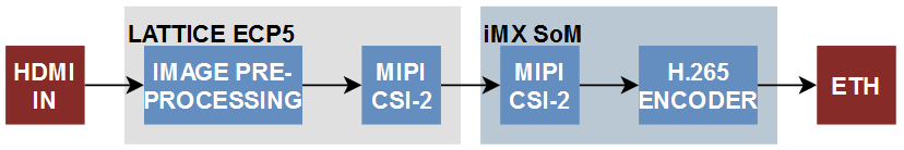
Hybrid video capturing and processing device
Lattice, ECP5, HDMI, MIPI, H.265
Video stream capturing, h.265 compression, and streaming to the Internet. Lattice ECP5 used for video preprocessing and i.MX8 based SoM for compression, streaming, and user logic.
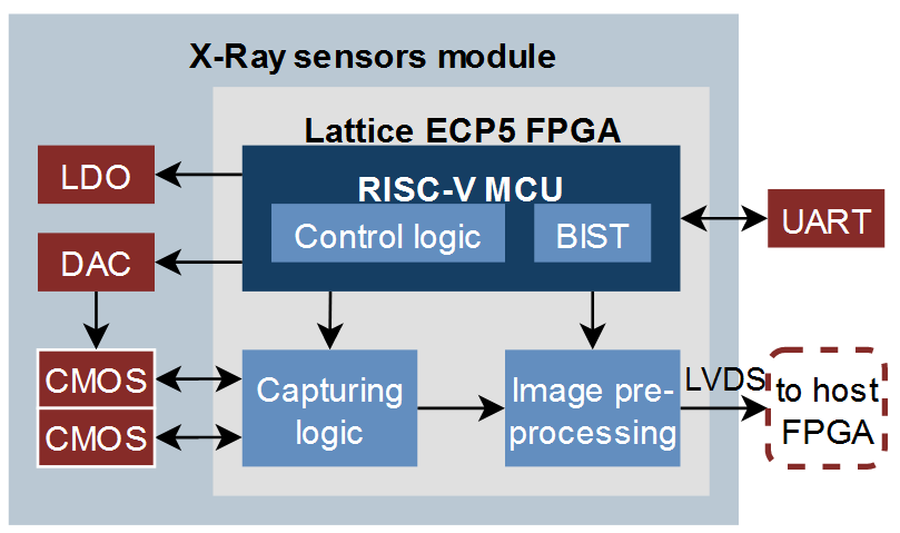
X-Ray sensors module
Lattice, ECP5, CMOS
A small PCB module with 2xCMOS sensors and Lattice ECP5 FPGA for control and image processing.
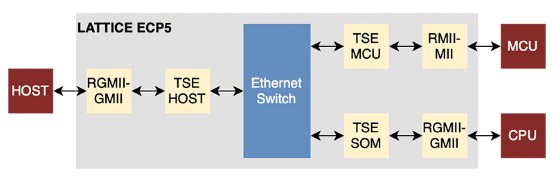
Simple L2 switch IP core
Lattice, Ethernet
A single physical Ethernet port shared between the embedded CPU and MCU SoM. The stream is routed on the base of the device’s MAC addresses.
Video decoding and output to TFT panel
Lattice, H.264, H.265 MIPI, Display
A video TS stream decoded by an iMX8 SoM module. Transmitted to Lattice FPGA using MIPI CSI-2 interface and displayed on the TFT panel.
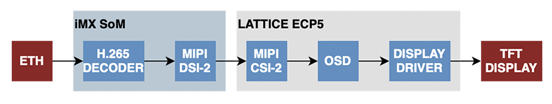
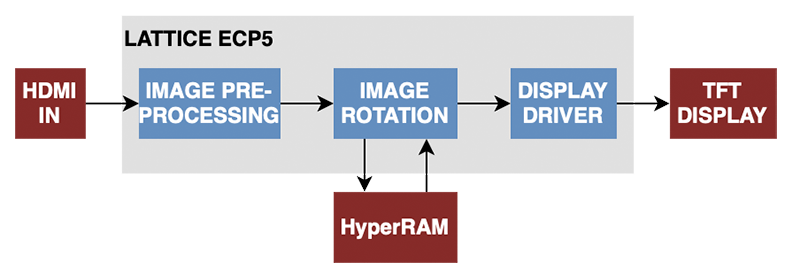
Image processing on ECP5
Lattice, Image Processing, HyperRam, Display
A video stream captured from HDMI interface. Then a chain of image processing operations takes place: white balance and gamma correction, cropping, scaling, and rotation. Finally, video displays on the TFT panel.
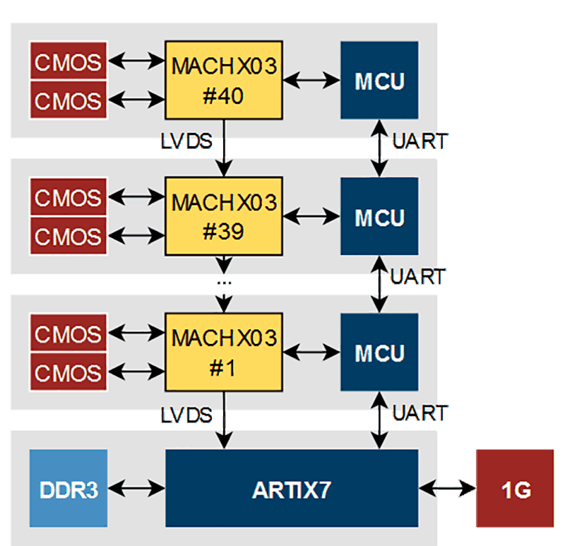
X-Ray imaging system
Lattice, CMOS, Xilinx, 1G
A complete device has been designed for image capturing from 80 X-Ray CMOS sensors. Image captured and pre-processed by Lattice MACHXO3 FPGA, downstream to ARTIX7 motherboard as daisy-chain. FW update and other control operations mediated by external MCU.
Microchip
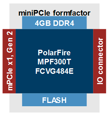
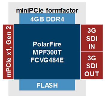
Polarfire mini-PCIe board
Microchip, Polarfire, Mini PCI-e
We designed a miniPCIe board with a Polarfire MPF300 FPGA. Key features:
- IO connector with MGTs
- 4 GB DDR4
- PCIe x1, Gen 2
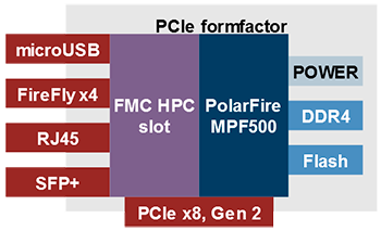
Polarfire PCIe FMC carrier board
Microchip, Polarfire, FMC, PCI-e
We designed a high-end processing board with a PolarFire MPF500 FPGA. Key features:
- 8 lanes of PCIe Gen2
- SPF+ cage
- FireFly x4
- Micro USB
- 16 GB DDR4
- FMC HPC connector
Polarfire mini-PCIe 3G-SDI card
Microchip, Polarfire, Mini PCI-e
We designed a miniPCIe 3G-SDI card with a PolarFire MPF300 FPGA. Key features:
- 3G-SDI recording and playback
- 4 GB DDR4
- PCIe x1, Gen 2
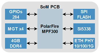
Polarfire SoM module
Microchip, Polarfire, SoM
We've designed a PolarFire MPF300 SoM module.
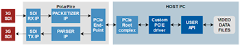
3G-SDI video capturing and playback
Microchip, Polarfire, SDI
FPGA firmware, host PC Linux driver, and API for 3G-SDI video streams capturing/playback.
NVidia
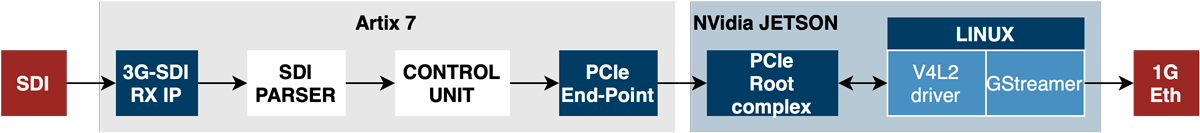
3G-SDI stream H.265 compression
Kintex7, Linux, PCI-e Jetson Nano, Drivers, H.265, SDI
The device compresses a 3G-SDI input stream with the H.265 encoder. A V4L2 driver adapts the PCIe data stream to be processed by GStreamer and NVidia HW codec. Linux controls the output bitrate by network throughput estimation (QoS). The PCIe links and delivers a low latency encoding chain.
Do you need a quote for your SoC FPGA design project?
Drop us a line about your project! We will contact you today or the next business day. All submitted information will be kept confidential.