


Why Edge AI Hardware That Wins the Demo Fails in Production
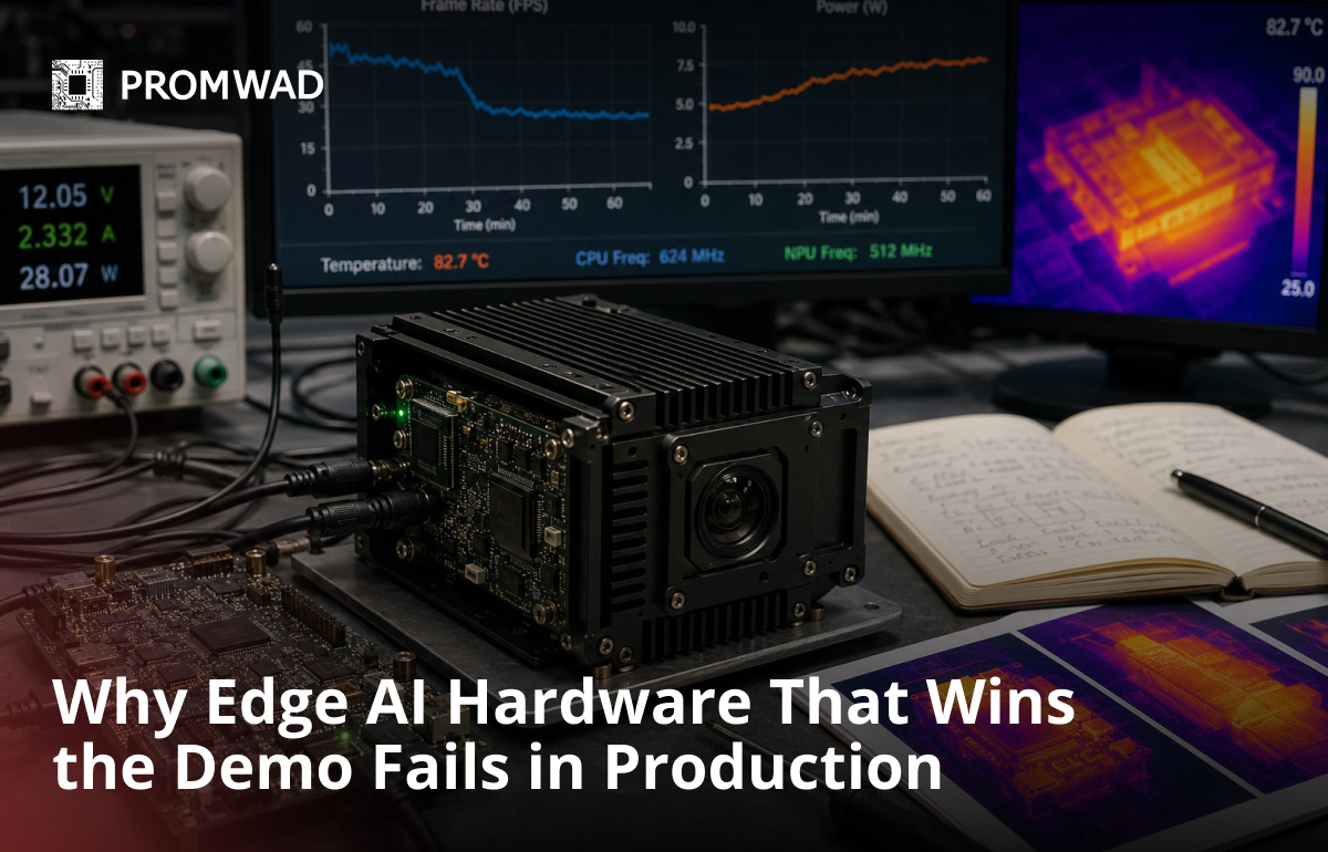
The module owned the demo. On the vendor's dev kit, the detection model ran at its target frame rate, the power reading looked comfortable, and the booth engineer had an answer for every question.
Months later the same silicon sat inside a sealed, fanless enclosure on a production line — same model, same clock, same input resolution. Frame rate held briefly, then settled well below target and stayed there. Sustained power ran over the module's budget. And the firmware team was finding that the next model revision no longer fit the memory budget the original evaluation had assumed.
Nothing in the silicon had changed. What had never been engineered was everything around it: the thermal path, the memory budget, the power envelope, and the model-update path. A demo answers one question — can this silicon run this model right now? Production asks a different one, and nobody had asked it yet.
Quick Overview
Problem: A vendor demo or eval-board result does not predict how an edge AI module behaves inside your enclosure, on your power budget, under sustained mixed workloads.
Common failure points: Thermal throttling when a sealed enclosure reaches steady state; external-memory traffic once the working set exceeds on-chip capacity; unsupported operators forcing execution fallback; peak TOPS that doesn't predict the real workload; working-set and accuracy changes across model revisions.
Where it appears: Industrial and machine vision, smart cameras, robotics perception, battery- or PoE-powered sensor nodes, automotive vision modules.
Engineering focus: Sustained-load and thermal validation, memory working-set budgeting, operator-coverage audit, power profiling across the duty cycle, OTA model lifecycle.
Wrong Assumption
The assumption behind most design-in disappointments is simple: if the module runs the workload in the demo, it will run it in the product. That skips the conditions a demo deliberately removes. A demo runs one curated model on an open dev board with active cooling and mains power, on clean input, for a few minutes. A product runs that same silicon in a sealed enclosure, on a battery or PoE budget, on messy field input, under a mix of concurrent tasks, sustained for hours, and re-flashed with new models across its service life. Peak TOPS, headline latency, and “runs AI on the edge” all survive the demo. Whether the module holds up under the product's thermal, memory, power, and lifecycle constraints is a separate question — and it is the one that decides the program.
Why It Fails
Peak TOPS rarely predicts production performance. Vendors specify theoretical accelerator throughput under defined precision, utilization, and dataflow assumptions. Actual batch-1 performance depends on operator mapping, memory traffic, preprocessing, runtime overhead, and concurrency, so headline TOPS is a poor predictor of how a specific model will run. What you observe: hardware chosen on peak TOPS or TOPS-per-dollar delivers a fraction of that on the real workload. Selecting the right edge AI platform is a system decision, not a peak-TOPS comparison.
Thermal behavior in the real enclosure. Eval boards run open-air with heatsinks and often a fan; a sealed, fanless enclosure reaches thermal steady state under sustained inference. Unless the thermal path is designed for that steady-state power, the SoC reduces its clock. What you observe: performance is stable for the first minutes of a run and degrades once the enclosure heats through. Holding it is a thermal and PCB problem — the domain of board-level thermal and power analysis.
Memory traffic, not just compute. When a model's weights, activations, or working set exceed the accelerator's effective on-chip memory capacity, additional external-memory traffic can turn bandwidth — not the MAC array — into the dominant latency constraint. What you observe: accelerator utilization stays low while latency targets are missed. This is the same memory-contention class documented in why AI inference latency fails in production.
Operator coverage and execution fallback. A vendor's NPU compiler supports a specific operator set. An unsupported operator may force part of the graph onto the CPU or another execution provider — or prevent compilation entirely — and even a small fallback subgraph can introduce synchronization and memory-copy overhead that dominates end-to-end latency. The demo model was chosen to map cleanly onto the NPU; your model may not. How operator coverage and CPU fallback affect real NPU performance is where this plays out in practice.
The model isn't frozen. Edge AI ships as software that gets revised and pushed over the air. A later revision — a larger architecture, a different precision or quantization scheme, higher input resolution, or added operators — can change the operator mix and push the working set past the memory budget validated during the original evaluation. Hardware sized to today's model leaves no headroom for the models the product will actually run.
In production these interact: a reduced clock, added external-memory traffic, and a fallback subgraph stack up under the exact concurrency the product runs at — and the module that led the demo misses spec on the line.
Hidden System Complexity
sensor → MIPI CSI / interface → ISP → memory → preprocessing → NPU / accelerator (on-chip vs. external-memory working set) → post-processing on host → actuation / transport → OTA model-update loop
The accelerator is one node on that path, and the datasheet describes only that node. A demo exercises the node in isolation; a product exercises the whole path under the enclosure's thermal ceiling and the system's power budget. A reduced clock, external-memory traffic, or a host-side post-processing stall all surface as “the AI is slow,” while the cause sits somewhere else on the path.
This is the same lesson as AI inference latency in real pipelines, pulled one layer down to hardware selection: the datasheet describes the accelerator under ideal conditions, not the system the product ships.
Failure Patterns
Scenario 1 (thermal). A vision module meets its frame-rate target on the open eval board. Sealed into a fanless production enclosure, it holds the target only briefly; as the enclosure reaches thermal steady state the clock is reduced, and sustained frame rate settles materially below target — in spec on the bench, out of spec in the field.
Scenario 2 (memory). A model meets its latency target during evaluation. A later revision increases the working set past the on-chip memory budget the evaluation assumed; external-memory traffic becomes the bottleneck and latency rises sharply on unchanged hardware.
Scenario 3 (operators). A model update introduces an operator the NPU compiler doesn't support. Part of the graph falls back to the host, which is already running preprocessing for several sensor channels, and end-to-end latency climbs under the concurrency the product actually runs at.
Edge AI Hardware Engineering
Edge AI production shortfalls — thermal throttling, external-memory traffic, unsupported operators, power overruns, no model-update headroom — are system-design problems, not demo problems. Closing them takes thermal and power co-design, memory working-set budgeting, operator-coverage validation, and an OTA-ready model lifecycle, not another benchmark on the dev kit. Promwad designs edge AI hardware, firmware, and system architecture — from NPU/SoC and carrier-board design to sustained-load validation and updatable inference pipelines.
Engineering Experience Across Edge AI and SoC Platforms






What Happens When Eval-Board Results Are Carried Into Production
Consider a typical edge-AI camera design. An SoC is selected after a strong eval-board demo — a detection model at the target frame rate, comfortable power on the open bench. Designed into a sealed, fanless production camera, the same module meets the target only until the enclosure reaches thermal steady state; the clock is then reduced and sustained throughput drops, while total power can exceed what the enclosure's thermal design allows for.
Two mechanisms typically compound here. The demo never reaches thermal steady state, but the enclosure does on every duty cycle, so the SoC crosses its throttle point. And a later model revision can push the working set past the on-chip memory budget the original evaluation assumed, so inference begins incurring external-memory traffic it did not before.
The engineering response is system-level rather than a model tweak: a thermal path and PCB stack-up designed for the workload's steady-state power, a model and quantization plan that keeps the working set within the validated memory budget, and a power profile validated across the real duty cycle rather than a bench burst.
Promwad builds production edge-AI camera hardware of this kind — see, for example, our AI camera platform on an Ambarella CVflow SoC. That project demonstrates production camera and SoC integration; the pattern above is a general design-in risk, not a description of that specific engagement.

Solution Approach
Step 1: Validate under sustained load and real thermals, not a bench burst. Run the target model in the production enclosure (or a thermal-equivalent fixture) to steady-state temperature and measure sustained frame rate, rail-level power, junction or board temperature, and operating frequencies after thermal steady state — not in the first minutes. The sustained numbers are the ones that matter. Where deterministic latency is critical, an FPGA-based datapath can provide more explicitly scheduled timing and lower jitter than a shared CPU/GPU software stack — though it still requires thermal, power, and memory-bandwidth validation at system level.
Step 2: Budget the memory working set before choosing silicon. Size the model's weights, activations, and working set — at production precision, and with headroom for future revisions — against the accelerator's effective on-chip memory. Where it doesn't fit, treat external-memory bandwidth as the real latency driver, or choose a part with more capacity. Confirm operator coverage against the vendor compiler for the actual model, not a reference network.
Step 3: Design the power and update path for the whole service life. Profile power across the real duty cycle (not peak), size it to the battery, PoE, or harvested budget, and build the model-update path — memory headroom, versioned or A/B model slots, rollback, validation — so future changes in architecture, precision, input resolution, or operator mix do not outgrow the deployed hardware. Choosing the platform itself is where these constraints should be decided, before design-in.
A demo answers whether the silicon can run a model once, under conditions chosen to flatter it. Whether the system can run and update that model across its service life is a separate, system-level question — a design step, not a benchmark.
Validation area | Demo condition | Production |
|---|---|---|
| Thermal | Open board, short run | Enclosure, thermal steady state |
| Memory | Reference model | Production model + headroom for revisions |
| Operators | Vendor demo network | Actual compiled graph on the target compiler |
| Power | Average board reading | Rail-level, full duty-cycle profile |
| Updates | Static image | Versioned or A/B model update with rollback |
Real Trade-Offs
Quantizing further — for example INT8 to INT4 — can shrink weights and cut external-memory traffic, but it may require quantization-aware training, may affect accuracy, and only delivers a benefit when the target accelerator and compiler support the lower precision efficiently.
A dedicated NPU can cut power draw versus GPU inference, but its operator coverage is narrower; an unsupported layer may force a fallback that erases the latency gain.
A sealed, passively cooled enclosure improves reliability and ingress rating, but may limit the sustained clock unless the thermal path is designed for the workload's steady-state power; active cooling recovers headroom at the cost of a failure point and added power and acoustic budget.
A heterogeneous SoC (CPU + NPU + real-time cores) runs control and inference on one part but makes every tenant share memory bandwidth; a discrete accelerator isolates the AI workload but reintroduces interconnect transfer cost and board area.
Headroom for future models costs money now — a larger-memory part is more expensive per unit but avoids a re-spin when the model grows. That ceiling is easier to judge with an experienced carrier-board and module design view of where the platform tops out.
Typical Edge AI Engineering Tasks

Sustained-Load & Thermal Validation
Running target models to thermal steady state in the production enclosure, measuring post-throttle frame rate and power, and defining the real duty-cycle envelope.
Memory & Operator Budgeting
Sizing the model working set against effective on-chip memory at production precision, auditing operator coverage against the vendor compiler, and planning external-memory bandwidth where the working set spills.
Hardware & Carrier-Board Design
SoC/NPU selection, carrier and module design, and thermal-aware high-speed PCB layout for edge AI hardware.
OTA Model Lifecycle
Memory headroom, versioned or A/B model slots, rollback, and revision validation so model updates don't outgrow the deployed hardware.
Qualifying Symptoms
- Performance meets target for the first minutes of a run and degrades once the enclosure reaches steady-state temperature.
- Sustained power runs over budget even though peak or burst power looked fine in the demo.
- Accelerator utilization stays low while latency targets are missed — a memory-traffic or fallback signal, not a compute limit.
- Hardware was selected on peak TOPS or TOPS-per-dollar, and achieved throughput on the real workload is a fraction of it.
At this point the work is system-level edge AI engineering, not another dev-kit benchmark. In practice: sustained-load and thermal validation in the real enclosure, memory working-set and operator budgeting against the actual model, power profiling across the duty cycle, and an OTA-ready model lifecycle.
For products where inference is one real-time tenant among control and I/O, the MCU firmware and RTOS layer and the embedded Linux and kernel layer are where scheduling and memory behavior are actually decided. And when the workload is industrial vision, the failure and its fix usually live in machine-vision system engineering, not in the model.
Promwad's public edge AI portfolio spans an Ambarella CVflow camera platform for vehicle access, an Infineon PSoC-based predictive-monitoring device (Ventisight), and an FPGA-plus-embedded-Linux multi-sensor rail platform. Across vision, sensing, and real-time processing, these are shipped hardware, firmware, and system-integration projects on different edge AI architectures — the same design-in and validation work this article describes.
FAQ
Why does my edge AI module hit its numbers in the demo but miss them in the product?
What is peak TOPS, and why is it misleading?
Why can the same task get slower after a model update on the same hardware?
When does an FPGA make more sense than an NPU or GPU for edge AI?
Related Engineering Cases
- AI Camera Platform for Vehicle Access: Edge AI vision on an Ambarella CVflow SoC; production camera and SoC/module integration.
- Predictive Edge-AI Monitoring for Ventilation Systems: Edge-AI analytics on embedded hardware in a deployed industrial product.
- Real-Time Rail Safety Platform for Multi-Sensor Data: FPGA plus multi-sensor fusion and edge AI analytics under sustained low-latency load.