AMD Zynq™ UltraScale+™ MPSoC and FPGA Design Services
As an FPGA design firm, we specialise in SoC-based hardware development with unmatched integration opportunities to provide robust performance.
Our partnerships give us access to leading technologies, including Zynq UltraScale+ MPSoCs and Kria™ SoMs.

Daniil Samoshchenko, Head of Partnerships at Promwad
About Zynq UltraScale+ MPSoC
The Zynq UltraScale+ MPSoC family combines a feature-rich 64-bit quad-core or dual-core Cortex-A53, dual-core Cortex-R5-based processing system, and programmable logic in a single device. These products include on-chip memory, multiport external memory interfaces, and a rich set of peripheral connectivity options.
Target markets: surveillance, computer vision, 5G wireless communications, augmented reality (AR), advanced driver-assistance systems (ADAS), industrial IoT, medical imaging
Our FPGA Design Services
Our Projects
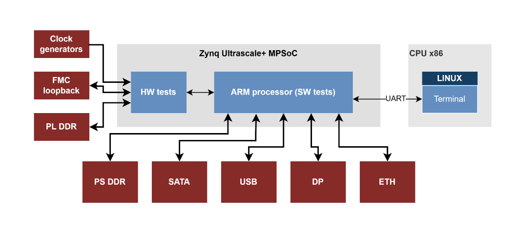
Automated At-Factory Tests for FPGA-Based Boards
Tags: Zynq UltraScale+ MPSoC, FMC, SATA, DDR, USB
We provided full life cycle support in FPGA-based board design. Our team developed firmware for at-factory automated tests based on Zynq UltraScale+ MPSoC boards. The automated tests cover all external PL and PS interfaces. The tests include DDR memory (PL and PS), FMC high-speed and low-speed lines, SATA, USB, clocking, etc.
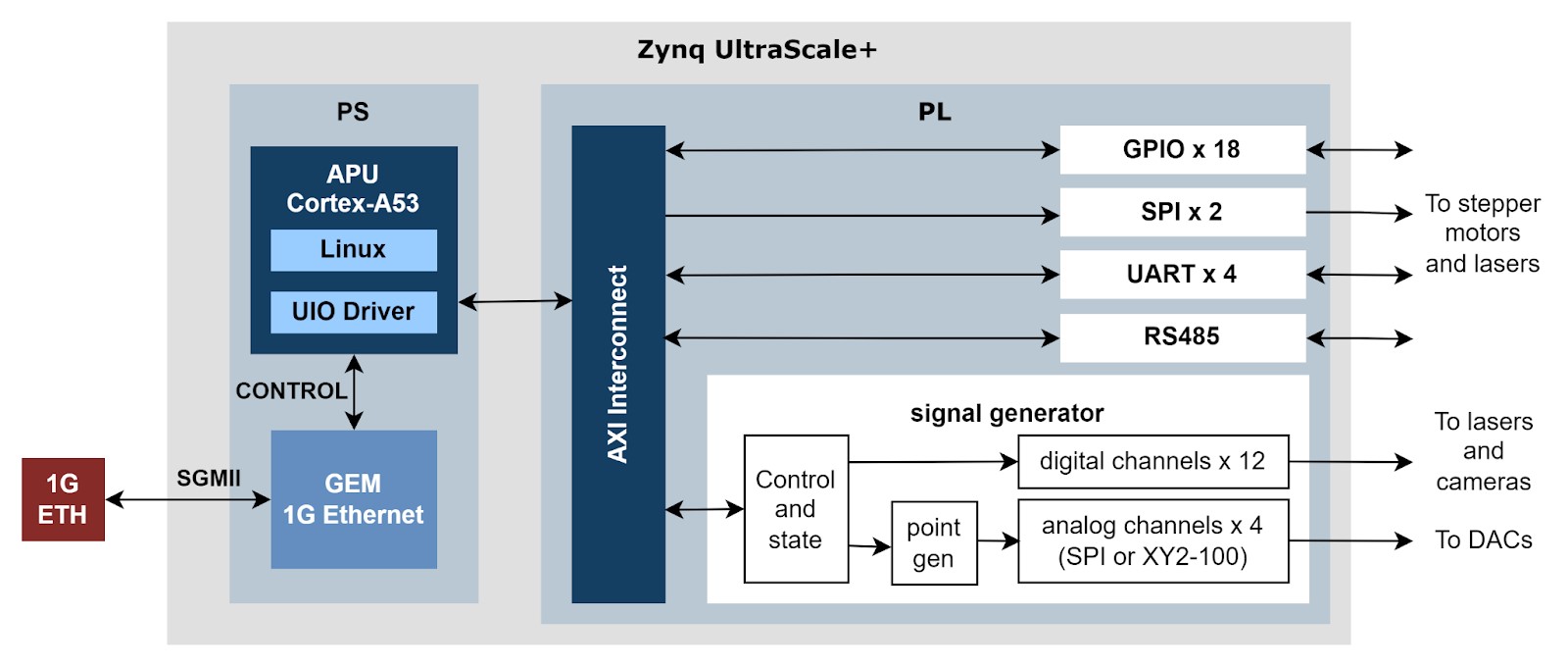
Firmware and Software Development of FPGA-Based Microscope
Tags: Zynq UltraScale+ MPSoC, Linux, Driver, SPI, XY2-100
Development of simple microscope firmware and software including signal generator for driving 2D scanners. Additional requirement was a software update opportunity for our customer's service, which is capable of updating the microscope firmware including the FPGA bit file. Signal generator provides automatic intermediate points generating using a second degree polynomial for analog channels.
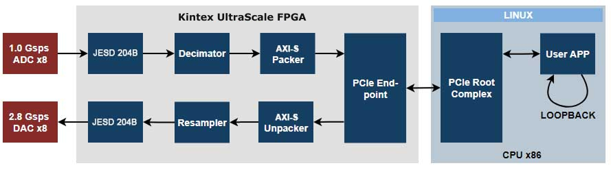
ADC/DAC Repeater
Tags: AMD Kintex™ UltraScale™ FPGA, MicroTCA, JESD 204B, Linux, PCIe
We designed firmware for the MicroTCA system for buffering data from ADC in CPU x86 system and translating it to the DAC.– 1 Gsps ADC x8 channels– 2.8 Gsps DAC x8 channels– DMA– PCIe
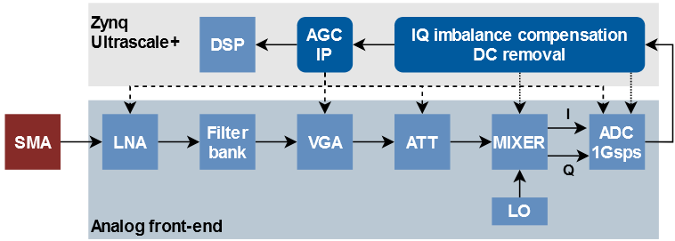
Analog Frontend Real-Time Controller
Tags: Zynq UltraScale+ MPSoC, SDR, AGC, IQ, AFE
AGC, IQ imbalance compensation, and DC removal algorithms have been implemented in Zynq Ultrascale+. The IP cores and software controls analog frontend board ICs provided parameters in real-time. AGC is table-based. IQ and DC techniques use surrogate optimization algorithm over ADC and mixer tunable parameters.
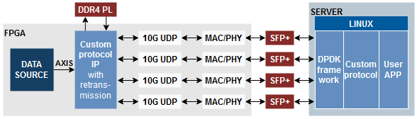
High-Speed Reliable Data Transfer over 4x10G
Tags: Zynq UltraScale+ MPSoC, DPDK, 10G, UDP, DDR4
A reliable data transfer chain from FPGA to a server with overall bandwidth up to 38 Gbps has been implemented. The DPDK framework used a server-side to allow high-rate data reception. A custom protocol with a retransmission feature has been implemented. The data cached in DDR4 PL external memory.
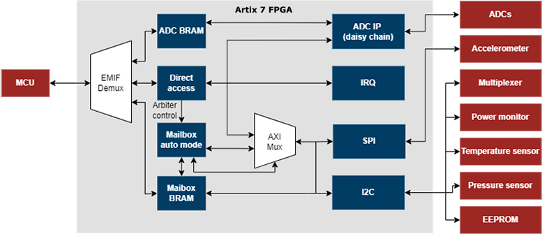
Interface Extension FPGA Project
Tags: AMD Artix™ 7 FPGA, MCU, ADC, SPI, I2C
- big-endian and little-endian support for EMIF
- direct access mode for MCU to end-points
- auto mode for polling end-points in round-robin
- arbiter switch for changing modes of access
- ADC controller with daisy chain support and internal configurable median filter
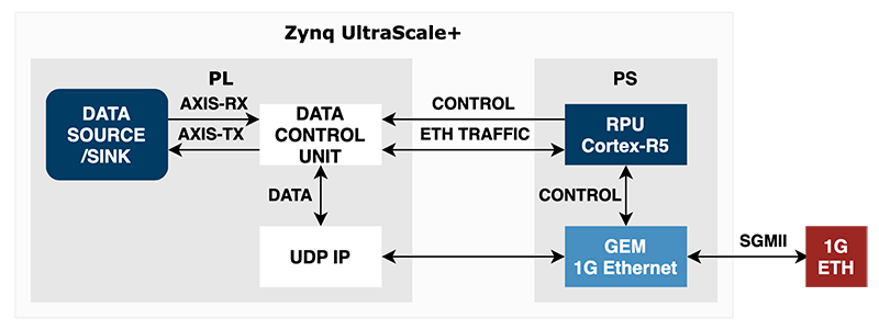
Zynq UltraScale+ MPSoC 1G Ethernet
An implementation of the UDP protocol with a hardware Gigabit Ethernet controller (GEM). Data is transmitted from both the PL and PS subsystems.
- Hardware UDP offloader
- AXI4-Stream data interfaces
- Control driver for RPU
- Packets routing between PL and PS using IP port
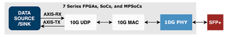
Zynq UltraScale+ 10G Ethernet
A hardware implementation of UDP protocol and 10G MAC.
- Hardware 10G UDP offloader
- AXI4-Stream data interfaces
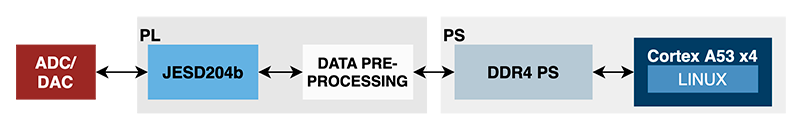
JESD204b Data Transfer to Linux
A design for high-speed ADC and DAC capturing and streaming from/to PS DDR4 memory. The subsystem runs under Linux application control.
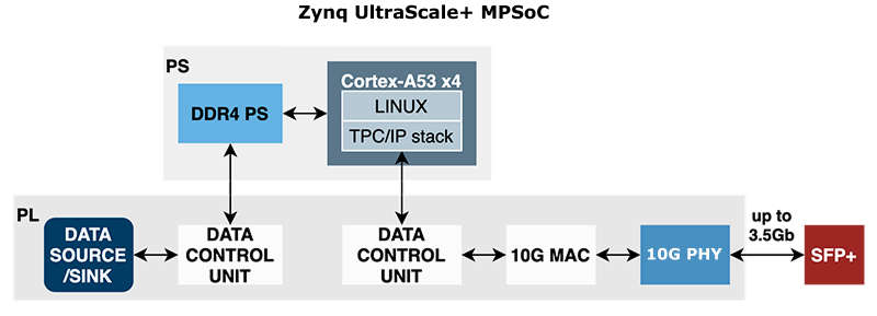
10G TCP/IP Using Linux
The design solves the problem of reliable data transfer from PL to server. Data transferred directly from PS DDR4 via TCP/IP protocol. The achieved bandwidth is 3.5Gb over a 10G interface.
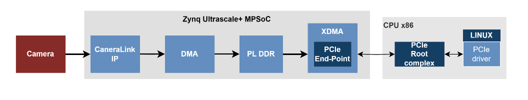
CameraLink Video Grabber
Tags: CameraLink, Zynq UltraScale+ MPSoC, Linux, PCIE driver, video grabber
We developed a video grabber from two CameraLink interfaces with the support of four modes: base (2.04 gbps), medium (4.08 gbps), full (5.44 gbps), and extended (6.8 gbps). We used a double-buffering mechanism in PL DDR memory for robust data transfers. The specific gearbox was developed to pack data from the camera to frames.
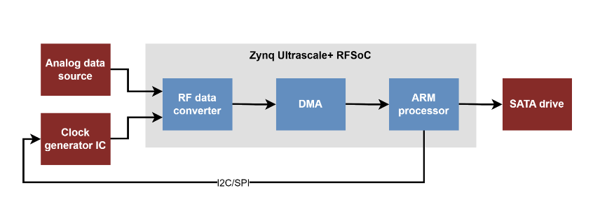
RFSoC ADC Data Capture
Tags: AMD Zynq™ UltraScale+™ RFSoC, ADC, SATA, SDR, I2C, SPI
We developed an ADC data capture system based on the Zynq UltraScale+ RFSoC. It captures data from three ADC channels, transfers it to the PS, and stores it on a SATA drive. The key challenge was ensuring gapless data transfer from PL to PS. In addition to data capturing, the Arm software configures the clocking subsystem via I2C and SPI interfaces. Zynq UltraScale+ RFSoC is a single-chip adaptable radio platform combining programmable logic, ADCs, and DACs on a single device.
Benefits of Zynq Ultrascale+ for FPGA Design
Performance
The solution surpasses the 700 Series devices up to 5X in performance and provides the best performance-per-watt on the market due to heterogeneous workload distribution and memory bandwidth.
Productivity
Zynq UltraScale+ devices provides a familiar environment for C/C++ developers, OS support, and quick implementation by reference design thereby increasing software and hardware development productivity.
Optimization
Zynq UltraScale+ features innovative ARM + FPGA architecture, extensive OS, middleware, stacks, accelerators, and IP ecosystem. The solution enables multiple levels of hardware and software security.
Processing System (PS)
Arm Cortex-A53 Based Application Processing Unit (APU)
-
Quad-core or dual-core
-
CPU frequency: Up to 1.5GHz
-
Extendable cache coherency
-
Armv8-A Architecture
-
64-bit or 32-bit operating modes
-
TrustZone security
-
A64 instruction set in 64-bit mode, A32/T32 instruction set in 32-bit mode
-
- NEON Advanced SIMD media-processing engine
-
Single/double precision Floating Point Unit (FPU)
-
CoreSightTM and Embedded Trace Macrocell (ETM)
-
Accelerator Coherency Port (ACP)
-
AXI Coherency Extension (ACE)
-
Power island gating for each processor core
-
Timer and Interrupts
- Arm Generic timers support
- Two system level triple-timer counters o One watchdog timer
- One global system timer
- Caches
- 32KB Level 1, 2-way set-associative instruction cache with parity (independent for each CPU)
- 32KB Level 1, 4-way set-associative data cache with ECC (independent for each CPU)
- 1MB 16-way set-associative Level 2 cache with ECC (shared between the CPUs)
Dual-core Arm Cortex-R5 Based Real-Time Processing Unit (RPU)
- CPU frequency: Up to 600MHz • Armv7-R Architecture
- A32/T32 instruction set
- Single/double precision Floating Point Unit (FPU)
- CoreSightTM and Embedded Trace Macrocell (ETM)
- Lock-step or independent operation
- Timer and Interrupts:
- One watchdog timer
- Two triple-timer counters
- Caches and Tightly Coupled Memories (TCMs)
- 32KB Level 1, 4-way set-associative instruction and data cache with ECC (independent for each CPU)
- 128KB TCM with ECC (independent for each CPU) that can be combined to become 256KB in lockstep mode
On-Chip Memory
-
256KB on-chip RAM (OCM) in PS with ECC
-
Up to 36Mb on-chip RAM (UltraRAM) with ECC in PL
-
Up to 35Mb on-chip RAM (block RAM) with ECC in PL
-
Up to 11Mb on-chip RAM (distributed RAM) in PL
Arm Mali-400 Based GPU
-
Supports OpenGL ES 1.1 and 2.0
-
Supports OpenVG 1.1
-
GPU frequency: Up to 667MHz
-
Single Geometry Processor, Two Pixel Processors
-
Pixel Fill Rate: 2 Mpixels/sec/MHz
-
Triangle Rate: 0.11 Mtriangles/sec/MHz
-
64KB L2 Cache
-
Power island gating
Platform Management Unit
-
Power gates PS peripherals, power islands, and power domains
-
Clock gates PS peripheral user firmware option
External Memory Interfaces
- Multi-protocol dynamic memory controller
- 32-bit or 64-bit interfaces to DDR4, DDR3, DDR3L, or LPDDR3 memories, and 32-bit interface to LPDDR4 memory
- ECC support in 64-bit and 32-bit modes
- Up to 32GB of address space using single or dual rank of 8-, 16-, or 32-bit-wide memories
- Static memory interfaces
- eMMC4.51 Managed NAND flash support o ONFI3.1 NAND flash with 24-bit ECC
- 1-bit SPI, 2-bit SPI, 4-bit SPI (Quad-SPI), or two Quad-SPI (8-bit) serial NOR flash
8-Channel DMA Controller
-
Two DMA controllers of 8-channels each
-
Memory-to-memory, memory-to-peripheral, peripheral-to-memory, and scatter-gather transaction support
Serial Transceivers
- Four dedicated PS-GTR receivers and transmitters supports up to 6.0Gb/s data rates
- Supports SGMII tri-speed Ethernet, PCI Express® Gen2, Serial-ATA (SATA), USB3.0, and DisplayPort
Dedicated I/O Peripherals and Interfaces
- PCI Express — Compliant with PCIe® 2.1 base specification
- Root complex and End Point configurations
- x1, x2, and x4 at Gen1 or Gen2 rates
- SATA Host
- 1.5, 3.0, and 6.0Gb/s data rates as defined by SATA Specification, revision 3.1
- Supports up to two channels
- DisplayPort Controller
- Up to 5.4Gb/s rate
- Up to two TX lanes (no RX support)
- Four 10/100/1000 tri-speed Ethernet MAC peripherals with IEEE Std 802.3 and IEEE Std 1588 revision 2.0 support
- Scatter-gather DMA capability
- Recognition of IEEE Std 1588 rev.2 PTP frames o GMII, RGMII, and SGMII interfaces
- Jumbo frames
- Two USB 3.0/2.0 Device, Host, or OTG peripherals, each supporting up to 12 endpoints
- USB 3.0/2.0 compliant device IP core
- Super-speed, high- speed, full-speed, and low-speed modes
- Intel XHCI- compliant USB host
- Two full CAN 2.0B-compliant CAN bus interfaces o CAN 2.0-A and CAN 2.0-B and ISO 118981-1 standard compliant
- Two SD/SDIO 2.0/eMMC4.51 compliant controllers
- Two full-duplex SPI ports with three peripheral chip selects
- Two high-speed UARTs (up to 1Mb/s)
- Two master and slave I2C interfaces
- Up to 78 flexible multiplexed I/O (MIO) (up to three banks of 26 I/Os) for peripheral pin assignment
- Up to 96 EMIOs (up to three banks of 32 I/Os) connected to the PL
Interconnect
-
High-bandwidth connectivity within PS and between PS and PL
-
Arm AMBA® AXI4-based
-
QoS support for latency and bandwidth control
- Cache Coherent Interconnect (CCI)
System Memory Management
-
System Memory Management Unit (SMMU)
- Memory Protection Unit (XMPU)
Configuration and Security Unit
- Boots PS and configures PL
- Supports secure and non-secure boot modes
System Monitor in PS
- On-chip voltage and temperature sensing
Programmable Logic (PL)
Configurable Logic Blocks (CLB)
-
Look-up tables (LUT)
-
Flip-flops
-
Cascadable adders
36Kb Block RAM
-
True dual-port
-
Up to 72 bits wide
-
Configurable as dual 18Kb
UltraRAM
-
288Kb dual-port
-
72 bits wide
-
Error checking and correction
DSP Blocks
-
27 x 18 signed multiply
-
48-bit adder/accumulator
-
27-bit pre-adder
Programmable I/O Blocks
-
Supports LVCMOS, LVDS, and SSTL
-
1.0V to 3.3V I/O
-
Programmable I/O delay and SerDes
JTAG Boundary-Scan
- IEEE Std 1149.1 Compatible Test Interface
PCI Express
- Supports Root complex and End Point configurations
- Supports up to Gen3 speeds
- Up to five integrated blocks in select devices
100G Ethernet MAC/PCS
- IEEE Std 802.3 compliant
- CAUI-10 (10x 10.3125Gb/s) or CAUI-4 (4x 25.78125Gb/s)
- RSFEC (IEEE Std 802.3bj) in CAUI-4 configuration
- Up to four integrated blocks in select devices
Interlaken
- Interlaken spec 1.2 compliant
- 64/67 encoding
- 12 x 12.5Gb/s or 6 x 25Gb/s
- Up to four integrated blocks in select devices
Video Encoder/Decoder (VCU)
- Available in EV devices
- Accessible from either PS or PL
- Simultaneous encode and decode
- H.264 and H.265 support
System Monitor in PL
-
On-chip voltage and temperature sensing
-
10-bit 200KSPS ADC with up to 17 external inputs
Zynq UltraScale+ MPSoCs
| CG Devices | EG Devices | EV Devices | |
| APU | Dual-core Arm Cortex-A53 | Quad-core Arm Cortex-A53 | Quad-core Arm Cortex-A53 |
| RPU | Dual-core Arm Cortex-R5 | Dual-core Arm Cortex-R5 | Dual-core Arm Cortex-R5 |
| GPU | – | Mali-400MP2 | Mali-400MP2 |
| VCU | – | – | H.264/H.265 |
More information about Zynq UltraScale+
The Zynq UltraScale+ MPSoCs are able to serve a wide range of applications including:
- Automotive: Driver assistance, driver information, and infotainment
- Wireless Communications: Support for multiple spectral bands and smart antennas
- Wired Communications: Multiple wired communications standards and context-aware network services
- Data Centers: Software Defined Networks (SDN), data pre-processing, and analytics
- Smarter Vision: Evolving video-processing algorithms, object detection, and analytics
- Connected Control/M2M: Flexible/adaptable manufacturing, factory throughput, quality, and safety
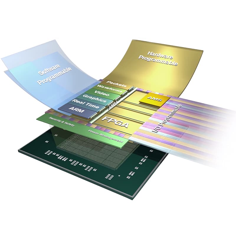
The UltraScale+ MPSoC architecture provides processor scalability from 32 to 64 bits with support for virtualization, the combination of soft and hard engines for real-time control, graphics/video processing, waveform and packet processing, next-generation interconnect and memory, advanced power management, and technology enhancements that deliver multi-level security, safety, and reliability. A large number of soft IP is available for the Zynq UltraScale+ MPSoC family. Stand-alone and Linux device drivers are available for the peripherals in the PS and the PL. AMD’s Vivado® Design Suite, Vitis™ unified software platform, and PetaLinux development environment enable rapid product development for software, hardware, and systems engineers. The Arm-based PS also brings a broad range of third-party tools and IP providers in combination with AMD’s existing PL ecosystem.
The Zynq UltraScale+ MPSoC family delivers unprecedented processing, I/O, and memory bandwidth in the form of an optimized mix of heterogeneous processing engines embedded in a next-generation, high-performance, on-chip interconnect with appropriate on-chip memory subsystems. The heterogeneous processing and programmable engines, which are optimized for different application tasks, enable the MPSoCs to deliver the extensive performance and efficiency required to address next-generation smarter systems while retaining backwards compatibility with the original Zynq-7000 SoC family. The architecture also incorporates multiple levels of security, increased safety, and advanced power management, which are critical requirements of next-generation smarter systems. AMD’s embedded UltraFast™ design methodology fully exploits the ASIC-class capabilities afforded by the architecture while supporting rapid system development.
The inclusion of an application processor enables high-level operating system support, e.g., Linux. Other standard operating systems used with the Cortex-A53 processor are also available for the Zynq UltraScale+ MPSoC family. The PS and the PL are on separate power domains, enabling users to power down the PL for power management if required. The processors in the PS always boot first, allowing a software-centric approach for PL configuration. PL configuration is managed by software running on the CPU, so it boots similarly to an ASSP.
Our Tech Map in FPGA
Vitis/Vivado, Quartus Prime, Diamond, Libero, Matlab
NVidia Jetson, Alveo, OpenVINO, TensorFlow, Keras, Caffe
Verilog, VHDL, VivadoHLS, Simulink/HDL Coder, С/C++, Python
High-speed PCBs, DDR4, JESD204b, HDMI, SDI, SI, PI, Thermo modeling
Zynq UltraScale+, RFSoC, Cyclone10, ECP5, MPF500
AD9361, AD9371, ADRV9009, Radars, Custom AFE, Antenas
DPDK, UDP 10G, TCP 10G, TAPs, L1/L2 IP cores
1G, 10G, 25G/40G, 100G
Our Case Studies


Do you need a quote for your FPGA design project?
Drop us a line about your project! We will contact you today or the next business day. All submitted information will be kept confidential.