Why Edge AI Accelerators Fail Without Hardware-Software Co-Design
Production Failure Scenario
The NPU hit 85 TOPS on the vendor benchmark. The product target was 30 ms end-to-end latency on a 1080p detection workload.
In integration, end-to-end latency was 120 ms. The NPU utilization was 34%.
The accelerator was fast enough. The path from sensor to accelerator and back was not.
The team had benchmarked the inference engine. Nobody had modeled the memory transfer cost, the preprocessing burden, or the DMA contention between the ISP and the NPU on the shared LPDDR4 controller.
Quick Overview
Problem:
Common causes:
Where it appears:
Engineering focus:
Wrong Assumption
Teams typically assume: if the accelerator’s TOPS rating exceeds the inference compute requirement, the system will meet its latency target.
In reality: TOPS measures peak compute on warmed-up tensors. Production latency includes sensor data transfer, preprocessing, model input staging, DMA to the accelerator, inference, DMA back, and post-processing — all competing for the same memory bandwidth and often the same CPU cores.
Why It Fails
The first failure mechanism is memory bandwidth saturation. On a typical edge SoC, the CPU, ISP, display controller, and NPU share one LPDDR4 channel rated at 25–34 GB/s. A 1080p RGB uint8 frame consumes ~6 MB. At 30 fps, frame data alone — including read and write passes for preprocessing buffers — can consume 180–360 MB/s of LPDDR4 bandwidth before any AI compute starts. This is the same dynamic that drives AI inference latency to diverge from benchmark numbers in production systems: the model itself is rarely the bottleneck.
The second is preprocessing cost on the wrong compute domain. Color space conversion, normalization, and tensor reshaping often run on the CPU because the NPU does not support these operations. On an Arm Cortex-A55, a single 1080p frame preprocessing pass takes 8–15 ms — more than the inference itself on a quantized model.
The third is operator coverage gaps. NPU toolchains support a subset of ONNX operators. A single unsupported layer — a custom activation, a depth-wise convolution variant, a non-standard pooling — forces CPU fallback. That fallback runs serially, stalling the NPU and increasing end-to-end latency by 20–60% on typical detection models.
The fourth, often missed, is platform fit at the selection stage. Choosing the wrong accelerator class for the workload locks in a ceiling that no amount of co-design will lift — the practical comparison of Jetson, Kria, Coral, and other edge AI platforms is where most of these decisions should be re-examined before silicon is committed.
Each effect amplifies the next. Memory bandwidth saturation lengthens input staging. CPU preprocessing eats into the same cores that handle NPU dispatch. Operator fallback serializes the pipeline. The NPU ends up idling at 34% utilization while the system is still missing its timing target.
Hidden System Complexity
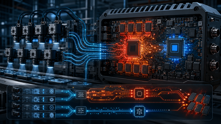
sensor → MIPI CSI → ISP → DMA to LPDDR4 → CPU preprocessing → DMA to NPU/FPGA → inference → DMA back → CPU post-processing → output
The NPU is one stage in this path. Its utilization depends on every stage upstream and downstream.
If the ISP writes frames at 30 fps but CPU preprocessing takes 18 ms per frame on a loaded core, the DMA buffer between ISP and CPU fills in 600 ms. After that, frame drops begin — not because the NPU is slow, but because the CPU cannot keep up.
The NPU stalls waiting for input. Utilization drops to 30%. End-to-end latency climbs while the accelerator benchmarks show peak performance.
This is a co-design failure. The memory layout, the DMA controller priority settings, the CPU core affinity for preprocessing threads, and the NPU dispatch scheduling must be designed together — not after the accelerator is selected. For workloads where deterministic latency matters more than peak throughput — sensor fusion, closed-loop control, multi-stream pre-processing — the architecture often shifts toward FPGA acceleration for AI applications precisely because it removes the scheduling-jitter problem at the source.
Failure Patterns
Scenario 1: Achieves target latency in single-stream mode at 30°C, fails under four concurrent camera streams when LPDDR4 bandwidth reaches 78% utilization and DMA transfers start queuing.
Scenario 2: Stable on quantized INT8 model during development, breaks after model update introduces one unsupported depthwise convolution layer that forces CPU fallback and adds 22 ms to each inference cycle.
Scenario 3: Passes vendor benchmark at 85 TOPS with synthetic tensors, fails in integration when preprocessing and ISP compete for the same LPDDR4 channel and effective NPU throughput drops to 28 TOPS under real camera load.
Edge AI Hardware-Software Co-Design Engineering
Edge AI failures in production are rarely model failures.
They are system failures — in memory bandwidth allocation, preprocessing scheduling, DMA topology, and operator coverage gaps that only appear when hardware and software are running together under real load.
Promwad designs FPGA, SoC, and embedded hardware for edge AI systems where inference, preprocessing, memory, and transport must be co-designed from the architecture phase.
Engineering Experience Across Edge AI and FPGA Platforms


A Multi-Camera Inspection System Where the Accelerator Was Not the Problem
A client building an industrial multi-camera inspection system had selected an NPU-integrated SoC with 40 TOPS. The detection model was quantized to INT8 and passed vendor benchmarks at 9 ms per inference. On paper, comfortably under budget.
In the integrated system, end-to-end latency landed at 75 ms against a 25 ms target for the reject control loop. The NPU ran at 38% utilization. Three weeks of model optimization gained nothing — predictably, because the model was not the bottleneck.
Analysis surfaced two compounding problems. Preprocessing for six camera streams consumed 60% of LPDDR4 bandwidth. The model included a custom attention layer that the NPU toolchain mapped to CPU fallback.
Replacing the preprocessing path with a hardware ISP pipeline and modifying the attention layer to use supported NPU operators brought end-to-end latency to 18 ms at 40% LPDDR4 utilization. The NPU was not replaced. The bottleneck had nothing to do with it.
Solution Approach
Step 1: Profile the full path under realistic load.
Instrument each pipeline stage — ISP, DMA, preprocessing, NPU dispatch, inference, post-processing — with timestamps under the actual camera count and frame rate. Measure LPDDR4 bandwidth utilization concurrently. The stage with the highest latency variance under load is where to focus first.
Step 2: Isolate memory and compute contention.
Run preprocessing alone and measure LPDDR4 utilization. Run inference alone. Run both concurrently. The delta reveals memory bandwidth contention. Run with and without other SoC tenants — display controller, connectivity stack, logging. Each tenant that shares the memory bus is a latency variable.
Step 3: Validate against p99, not mean, under thermal load.
Edge AI systems fail on tail latency, not average. Validate at p99 under sustained thermal soak at the rated operating temperature. An NPU that meets its target at 25°C and fails at 85°C has a power budget problem that no software optimization will fix.
Accelerator utilization below 60% while end-to-end latency is failing is the strongest signal that the bottleneck is outside the NPU — and the strongest argument for stopping model tuning and starting data-path analysis instead.
Real Trade-Offs
- Increasing NPU batch size improves throughput but increases p99 latency because frames wait for the batch to fill — unacceptable in closed-loop control systems with <30 ms requirements.
- Moving preprocessing into hardware (ISP pipeline, FPGA pre-processor) reduces CPU load and LPDDR4 bandwidth by 40–60%, but tightly couples the sensor interface, memory layout, and acceleration path — making future camera changes expensive.
- Choosing an NPU over FPGA reduces power by 40–60% for standard model architectures, but FPGA provides deterministic latency and full operator coverage — critical when models change frequently during product iteration. The trade-off space across Jetson, Kria, Rockchip, and Movidius for real-world edge AI workloads is sharper in 2026 than it was even a year ago, because transformer-heavy models change the operator-coverage equation.
- Quantizing from FP16 to INT8 cuts inference time and memory bandwidth by 2x, but requires quantization-aware retraining and validation against the calibration dataset — typically 2–4 engineering weeks.
- Prioritizing LPDDR4 bandwidth for the NPU through QoS settings reduces camera ISP write latency and can cause dropped frames at high frame rates on multi-camera systems.
Typical Edge AI Co-Design Engineering Tasks

Accelerator Architecture Selection
Evaluating NPU, FPGA, GPU, and CPU-based acceleration options against latency, power, operator coverage, and production deployment constraints for the specific model and workload.
Memory Bandwidth and DMA Topology Design
Modeling LPDDR bandwidth allocation across ISP, CPU, NPU, and display tenants; designing DMA priority and zero-copy buffer strategies to eliminate transfer bottlenecks.
Preprocessing Hardware Offload
Designing ISP-to-NPU preprocessing pipelines using hardware acceleration (FPGA, VPU, or ISP pipeline) to eliminate CPU preprocessing as the dominant latency source.
Model Deployment Validation
Validating model operator coverage against the target NPU toolchain, identifying CPU fallback paths, and restructuring unsupported layers to maintain NPU execution.
Qualifying Symptoms
- NPU or FPGA utilization stays below 60% while end-to-end inference latency exceeds the target.
- Latency target is met in single-camera mode and fails when two or more camera streams run concurrently.
- End-to-end latency increases by more than 30% when logging, telemetry, or network transmission run concurrently with inference.
- Model update that adds a new layer type causes latency to increase by 20+ ms without changing the accelerator.
- System meets latency target at room temperature and fails after 20 minutes of thermal soak.
- LPDDR4 or LPDDR5 bandwidth utilization exceeds 70% during inference under full sensor load.
- Post-processing on CPU causes the accelerator to stall between frames, visible as periodic latency spikes at regular intervals.
From here, the work is co-design analysis. Selecting a higher-TOPS accelerator will not move the needle until the data path is modeled end-to-end.
In practice this means: profiling the full sensor-to-output path under real load, modeling LPDDR bandwidth allocation across all SoC tenants, evaluating hardware preprocessing offload options, and validating the model deployment against actual NPU operator coverage.
A related layer of risk sits in the software stack itself — toolchain instability, BSP drift across SDK versions, and reproducibility gaps in the firmware that runs the NPU dispatch. When the system misses latency under load and the data-path looks clean, the next place to look is why embedded software toolchains break after board bring-up.
End-to-end, this is where edge AI engineering on the device becomes the difference between a system that meets its latency target and one that is waiting for a hardware revision.
This class of problem appears frequently in multi-camera industrial vision systems, robotics perception stacks, and embedded AI platforms where inference latency is part of a closed-loop control requirement. The same architecture trade-offs propagate down into low-power IoT sensor devices* when TinyML inference moves onto the MCU itself.*
Related Engineering Cases
Real-Time Rail Safety Platform for Multi-Sensor Data: FPGA + multi-sensor fusion + edge AI analytics for low-latency safety inference under sustained real-time load.High-Speed OpenGear Cards for Multi-Camera Broadcasting: FPGA-based high-speed video transport and processing — directly relevant to multi-stream edge AI workloads on shared memory subsystems.
FPGA-Based Video Decoding for Public Transport HMI: Deterministic video processing and AI inference pipeline for embedded transport displays.
FAQ
Why is NPU utilization low when the system is missing its latency target?
FPGA vs NPU for edge AI — when does each make sense?
Does INT8 quantization solve latency problems?
What is operator coverage and why does it matter?
How is co-design different from just selecting hardware?