How to Reduce EMI in Compact Industrial Electronics: PCB Layout and Shielding Tactics
Electromagnetic interference (EMI) is one of the most persistent challenges in industrial electronics design—especially when working with compact enclosures or densely populated PCBs. In 2025, as devices become more integrated and miniaturized, the risk of EMI-related failures increases dramatically, affecting signal integrity, certification, and even safety.
In this article, we explore practical engineering strategies to reduce EMI in embedded industrial systems, focusing on PCB layout, grounding, filtering, and shielding, as well as simulation tools that help engineers design right the first time.
Why EMI is a growing issue in compact devices
Modern embedded systems include high-speed interfaces (USB 3.x, HDMI, Ethernet), wireless modules (Wi-Fi, BLE, LoRa), switching regulators, and powerful MCUs or SoCs—all packed into smaller form factors. This increases the likelihood of:
- Crosstalk between high-speed signals
- Radiated emissions exceeding regulatory limits
- Power supply noise affecting analog and RF circuits
- Unexpected system resets or data corruption
Moreover, with the rise of Industry 4.0 and IIoT deployments, many devices operate near harsh industrial equipment, introducing external EMI sources as well.
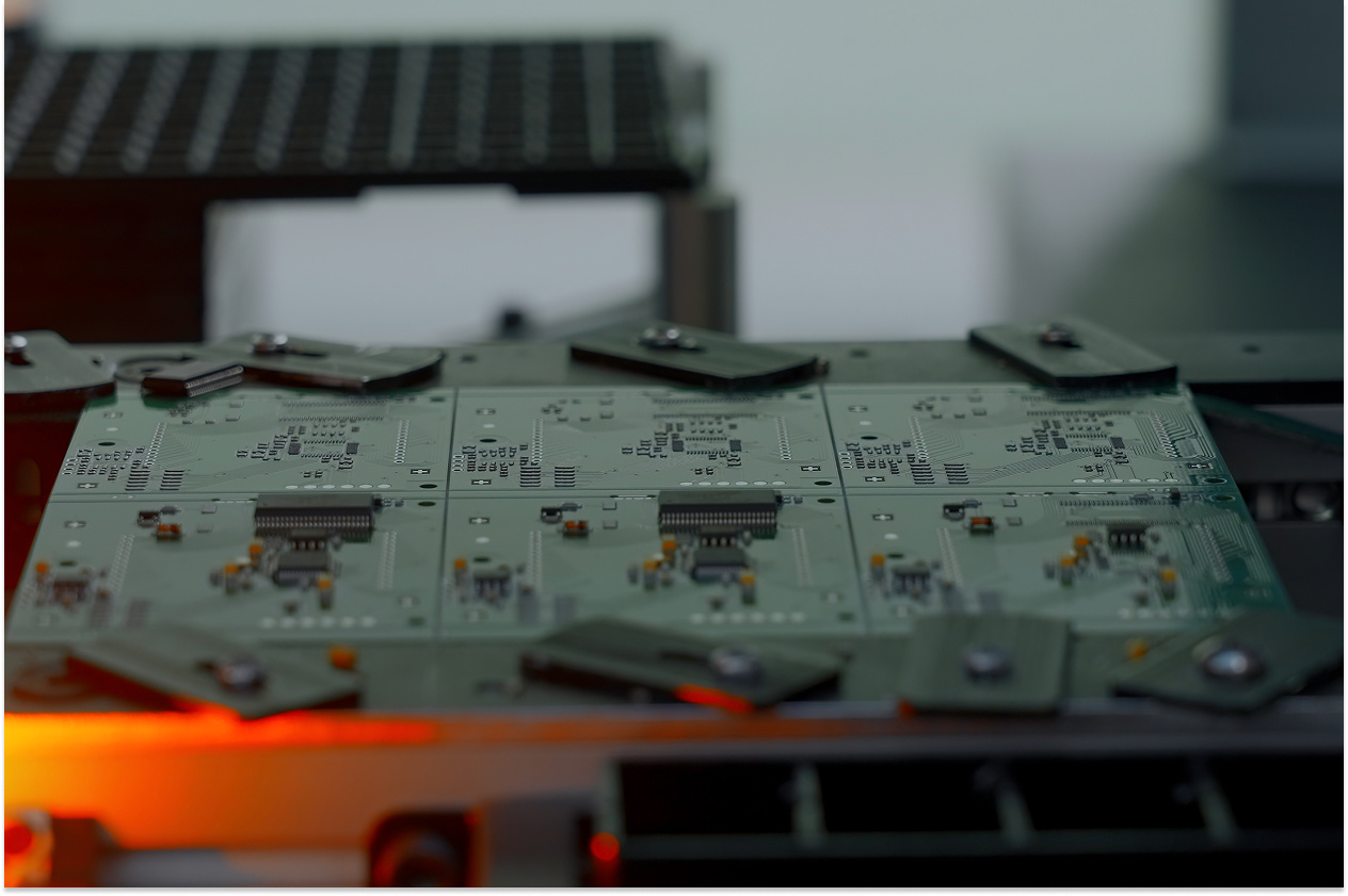
EMI design starts with the PCB layout
The PCB layout is the foundation of EMI performance. Good EMI behavior is often a result of planning, not patching.
Key layout techniques:
- Use continuous ground planes: Always route return paths directly beneath high-speed signal traces. Avoid breaks in the reference plane that force current to loop.
- Minimize loop areas: Keep current loops small—especially in high-speed or high-current paths. Loop antennas are a primary source of radiated EMI.
- Controlled impedance routing: Differential pairs (USB, Ethernet, LVDS) must be routed with controlled impedance and tight coupling. Avoid stubs or via stubs.
- Separate analog, digital, and power grounds properly: Use star grounding or hybrid approaches to reduce coupling between domains.
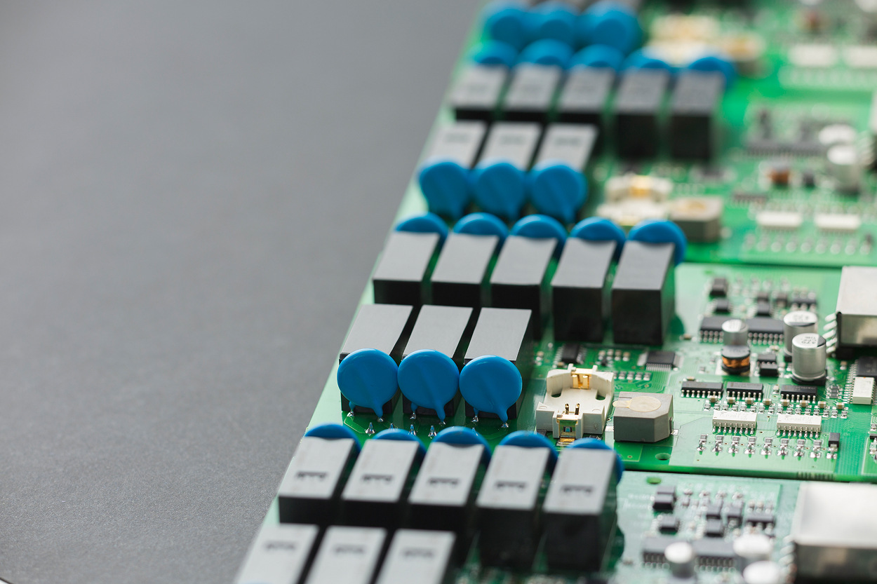
- Decouple at multiple levels: Place bulk capacitors at power inputs and small ceramic capacitors close to IC power pins. Use at least one decoupling cap per power pin.
- Use guard traces and stitching vias: Shield sensitive analog or RF traces with grounded guard traces. Stitching vias around high-frequency zones reduce emissions.
Filtering and power integrity
Filtering is essential to prevent conducted EMI through power or signal lines.
- Use LC filters on power inputs and outputs: Add pi filters or ferrite beads to reduce high-frequency noise.
- Common-mode chokes: These are particularly effective on differential interfaces like Ethernet or USB.
- Input ESD protection + EMI suppression components: TVS diodes, transient filters, and gas discharge tubes protect against spikes while reducing noise.
- Isolated power domains: In high-EMI environments, galvanic isolation for communication and power may be necessary (e.g., via isolated DC/DC or opto-isolators).
Shielding in compact enclosures
When space is limited, shielding must be planned together with mechanical design. Key approaches:
- Conductive enclosures: Use metal housings or apply conductive coatings to plastic enclosures.
- Board-level shields (cans): Place metal shields over critical ICs, especially RF transceivers, CPUs, and DC/DC converters.
- Gasket and seam management: Ensure electrical continuity between shield pieces. Poor grounding defeats the purpose.
- Cable shielding and connectors: Use shielded cables and connectors with 360° grounding for I/O. Poor cable design can act as an antenna.
Simulation and pre-compliance testing
To catch EMI issues early, simulation and modeling are essential.
- Signal Integrity (SI) and Power Integrity (PI) tools: Tools like HyperLynx, Ansys SIwave, or Keysight ADS help analyze high-speed behavior and impedance mismatches.
- EMC simulation: CST Studio Suite and EMPro can simulate radiation from the board or enclosure, identifying hot spots.
- Near-field scanning: During prototyping, use near-field probes and spectrum analyzers to locate sources of emission before final EMC lab testing.
Case study: EMI mitigation in IIoT gateway (Promwad)
In one recent Promwad project, our client faced EMI failures during certification of a compact IIoT gateway with Wi-Fi + Ethernet + CAN interfaces. We reduced emissions by:
- Revising the return path under Ethernet differential pairs
- Adding common-mode chokes and series damping resistors
- Redesigning the enclosure with a shielded sub-compartment
- Running simulation to validate impedance and emission profile
The result was a successful CE/FCC pre-certification pass, reduced redesign cycles, and faster time to market.
How Promwad supports EMI-aware electronics design
We assist clients in:
- EMI-conscious PCB stackup and layout design
- High-speed routing, impedance control, and simulation
- Power integrity and filtering analysis
- Shielded mechanical enclosure design
- Regulatory preparation: CE, FCC, CISPR, EN 55032
- SI/PI/EMC co-design for industrial and telecom products
Our team works closely across hardware and mechanical engineering to ensure compliance without costly redesigns.
Conclusion
In compact industrial electronics, EMI is no longer a secondary concern—it is a design constraint from day one. With proper layout, filtering, shielding, and simulation, you can dramatically reduce emissions, avoid certification failures, and ensure robust system behavior in real-world environments.
Need expert help with EMI design or debug? Let Promwad assist you in building compliant, compact, and reliable electronics for the most demanding industries.
Our Case Studies