Advanced Packaging Technologies: The Future of Chiplet Integration
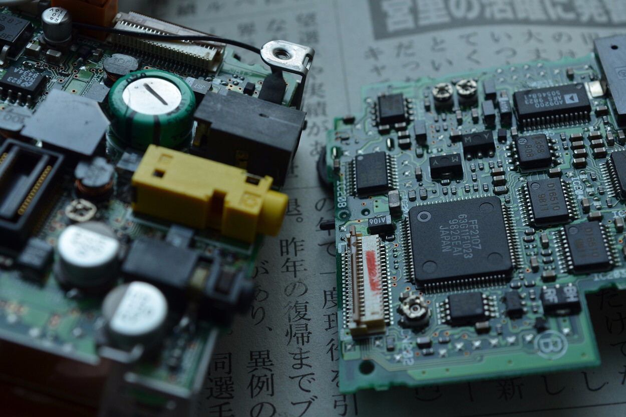
In the world of semiconductors, the age of monolithic chips is quietly giving way to something more flexible and powerful. Rather than sandwiching every feature into a single silicon die, engineers now build chips piece by piece—chiplets—using advanced packaging technologies to seamlessly connect them. Today, I’ll walk you through how this shift isn’t just a technical buzz but the foundation for smarter, scalable, and future-ready electronics.
What exactly makes advanced packaging such a game-changer for chiplet integration?
Think about a puzzle where each piece specializes in a function—one handles AI compute, another manages memory, and yet another interfaces with RF hardware. That’s essentially what chiplets offer. Now, adding advanced packaging to that mix transforms the puzzle into a compact, robust system. Techniques like 2.5D and 3D integration, fan-out wafer-level packaging, and hybrid bonding mean those pieces can be stacked or spread out with blazing-fast interconnects and efficient heat flow.
This modularity wasn’t possible years ago when manufacturing constraints forced designers to cram everything into a single die, often sacrificing yield or function. Now, with advanced interconnects like TSVs (through-silicon vias) and redistribution layers, performance leaps without ballooning costs or complexity. It also unlocks flexibility—designers can mix and match chiplets made on varying nodes or specialized processes, like combining a 3nm compute tile with older memory or analog chiplets—all within a single package.
Which real-world innovations show what advanced packaging makes possible?
Some real-world examples help ground the concept. TSMC is developing a system-on-wafer (SoW-X) packaging that places chiplets and high-bandwidth memory directly onto a full wafer, achieving performance-per-watt gains up to 65 percent. That’s not some distant lab experiment—it’s expected to ship by 2027 and hints at how chip integration will evolve in data centers and beyond.
Meanwhile, companies like Marvell are delivering modular RDL interposer platforms that make multi-die AI accelerator designs up to 2.8 times larger than conventional single-die designs—without a proportional jump in power or thermal hassles. Studies also show how folding chiplets on substrates like glass or specialized 2.5D arrangements can further improve performance density and substrate design flexibility.
Then there’s the industry response to geopolitical and supply chain complexities: chiplets let designers source components from diverse vendors and mix them at the package level, sidestepping reticle-size limitations and regional manufacturing bottlenecks.
What challenges still make advanced packaging tricky—and how are they being solved?
I won’t sugarcoat it: advanced packaging isn’t plug-and-play. Heat crowding, reliability under stress, and alignment challenges in packaging are real hurdles. For example, fan-out wafer-level packaging must carefully manage mismatches in thermal expansion or layer warping over time. Fault detection needs to be robust—certain recent methods embed built-in self-tests into packaging layers to detect misaligned chiplets or cracked interconnects during assembly.
Design is another headache. When parts come from different nodes or vendors, aligning performance, signal integrity, and physical packaging requires a holistic toolset—not just a stand-alone chip designer or PCB engineer. That’s why platforms like Integrated Design Ecosystems (IDE) aim to unify layout, routing, and verification workflows, dramatically reducing design cycle time.
Still, the trends are clear: foundries and packaging houses are investing billions. Samsung, for example, is building a $40 billion advanced packaging facility to lead in this space. Nvidia continues to ramp up demand for high-density CoWoS-L packaging from TSMC, even as packaging bottlenecks remain prominent concerns at the executive level.
How will advanced packaging reshape the future of semiconductor design?
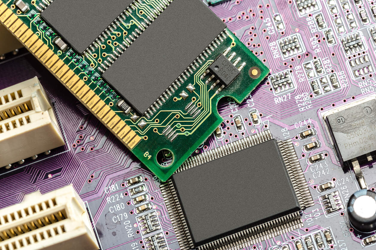
Think of a future where chips aren’t static, monolithic slabs but adaptive toolkits. High-performance AI engines stack next to memory, analog radios, or security modules—all inside a micro-scale package that fits your laptop or smartphone.
Within the next few years, I expect to see more varieties of packaging surface: silicon photonics and optical interconnects packaged close on die to scale AI bandwidth, fan-out packages that lower cost for mass-market devices, and standards like UCIe enabling chiplets from different vendors to plug into unified ecosystems.
Down the line, the idea of custom “app-defined” chiplets could emerge—imagine designing your own smartphone with CPU, radio, AI, and security tiles swapped in as you like, assembled in a standardized package at scale. That’s the modular future advanced packaging is building toward.
Right now, the hardware industry is facing a new frontier—guiding chip evolution through packaging innovation rather than raw transistor scaling. And for anyone in embedded, systems, or hardware design, chiplet-ready, packaging-first thinking isn’t optional—it’s the new normal. Let me know if you'd like to dive deeper into substrate-level innovations, thermal modeling, or emerging standards like UCIe.
Our Case Studies

