PCB Expert's View: Altium vs KiCad Productivity


The debate between Altium Designer and KiCad is often driven by their contrasting approaches: Altium's professional features and polished environment versus KiCad's open-source flexibility and cost benefits. To shed light on these differences, we share professional insights into how each platform affects day-to-day design, project costs and efficiency.
When it comes to PCB design, Altium Designer and KiCad are two of the most widely used tools, each with unique advantages and trade-offs.
Altium, a commercial software, is known for its extensive features, polished user interface and easy integration with libraries and production tools. On the other hand, KiCad, an open-source alternative, offers flexibility, cost-effectiveness and an active community, although it may lack some of Altium's top features.
I asked our PCB designers about the differences between the two platforms and how they affect workflow, project costs and design capabilities. They made a detailed comparison for this blog post, looking at features, usability, and suitability for different project types to help you make an informed decision.
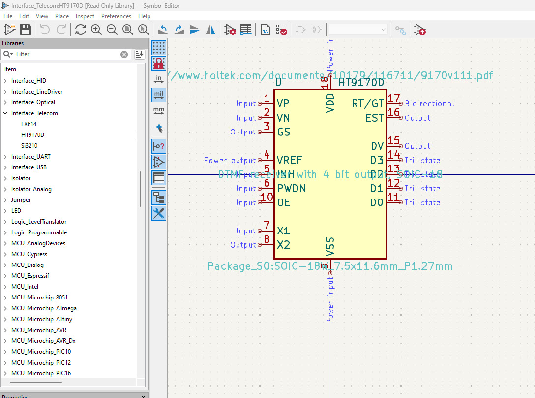
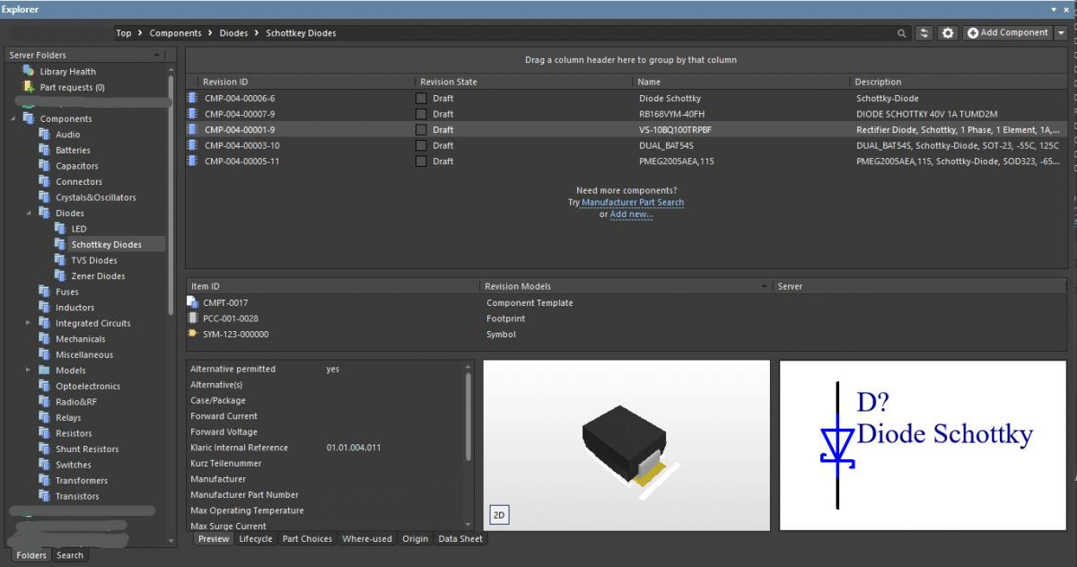
Symbol libraries
| KiCad | Altium |
| KiCad's included symbol library is accessible, well organised and easy to use. Perfect for a quick start. | Altium's database library can work with over 100,000 components distributed across all workspaces but requires quite a heavy initial setup. |
|
|
|
Footprint creation
| KiCad | Altium |
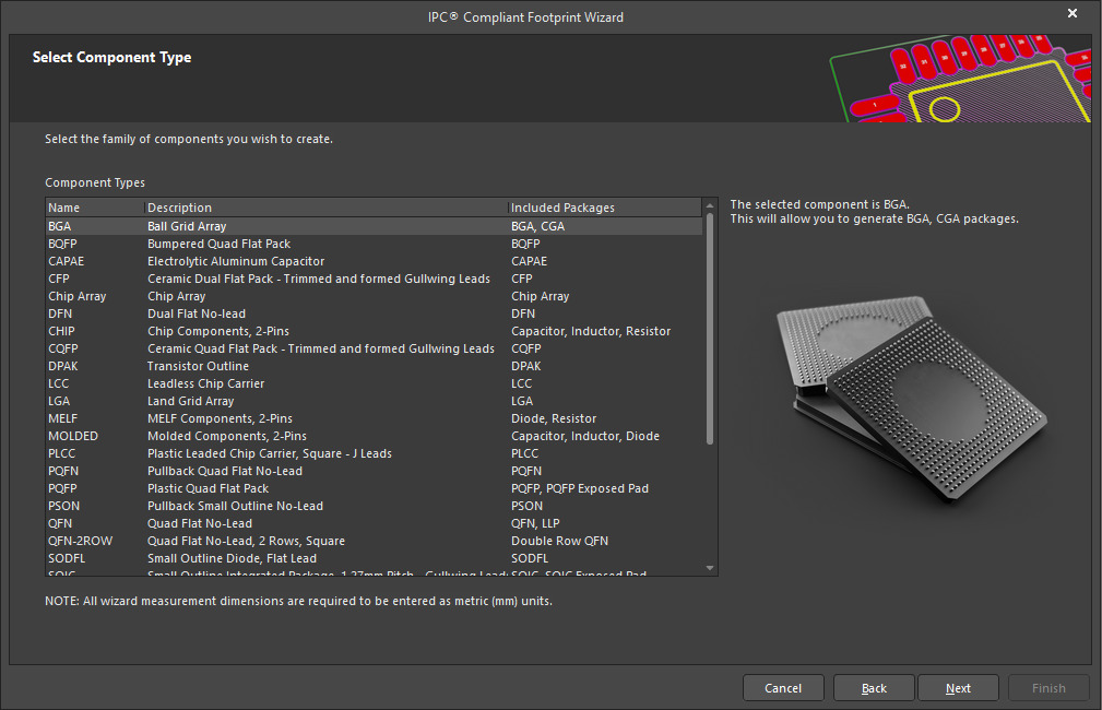
| The huge library is included in the package. You can create one using the standard workflow if you do not have a finished footprint. Test package: non-standard VFBGA-153 can be created in 12 minutes without plugins. | It has poor library without intuitive UI/UX, its major part must be loaded from the server. However, Altium has a powerful IPC footprint-compliant wizard that saves a lot of time. Test package: non-standard VFBGA-153 can be created in 4 minutes using the built-in wizard. |
|
|
|
Structure options
| KiCad | Altium |
| Vertical structure only. | It can be structured horizontally or vertically or with multiple channels. |
| | |
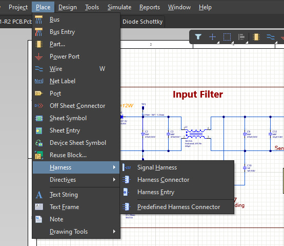
Schematic workflow for IoT and industrial projects
| KiCad | Altium |
| The toolset is sufficient for standard design. | Advanced schematic and internal interconnect toolset |
| | |
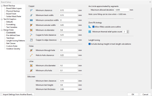
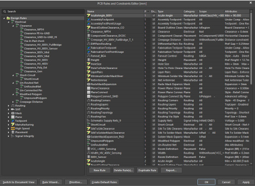
Constrain setup
| KiCad | Altium |
| Default constraint setup. | Advanced constraint setup. Advanced copper control. Creepages, DFM, and DFA pre-checks. Powerful query system. |
| | |
User interface
| KiCad | Altium |
| Simple and easy to use colour system. Good pre-defined layer data. Usually, no setup required. | Editing parameters must be set. The setup is advanced, but it makes a long initial setup much easier. |
|
|
|
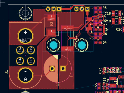
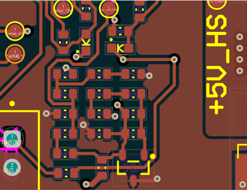
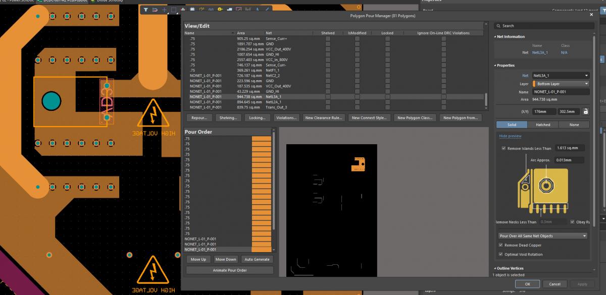
Copper management
| KiCad | Altium |
| A standard toolset for copper filling. | Advanced tools for polygon sorting, shape editing, and management. |
| | |

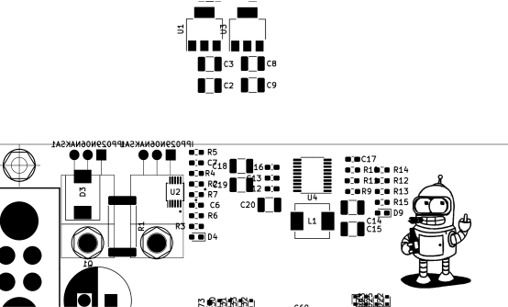
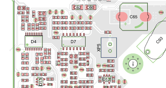
Assembly documents workflow
| KiCad | Altium |
| Its standard setup is similar to most other tools. | Altium has a draftsman that creates assemblies quickly and easily in just a few clicks. |
| | |
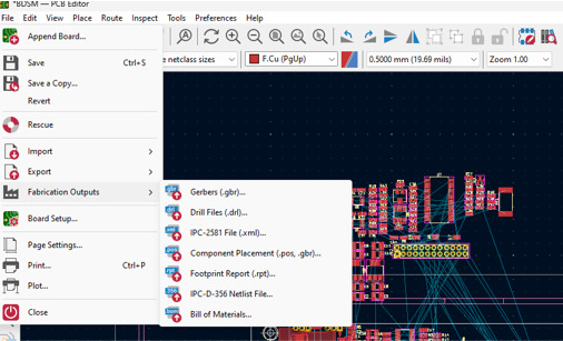
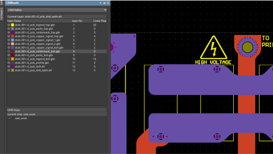
Manufacture documents workflow
| KiCad | Altium |
| Standard output export. | An advanced CAM processor included. |
| | |
Collaborative options
| KiCad | Altium |
|
|
The best choice between Altium Designer and KiCad depends on your project requirements. Altium is ideal for complex, large-scale or commercial projects that require advanced features, integrations and efficient collaboration. It's a top choice for professionals looking for stable capabilities for high-volume production.
In contrast, KiCad is well suited to mid-scale or hobbyist projects, start-ups on a budget, and those who prefer a flexible open-source platform. It may lack some advanced features, but it's a powerful tool for efficient, cost-effective PCB design.
Are you looking for expert guidance on choosing the right PCB design software for your project?
Case Studies in Hardware Design