


Why FPGA and MPSoC Broadcast Pipelines Fail Under Full Production Load

The design passed the bench. The datapath hit its channel count, latency looked comfortable, and the demo ran clean.
Then it ran as a full media chain on the production board. Under the full channel count, the datapath and the processor subsystem competed for shared interconnect and memory, and latency on the deterministic path began to wander. After a brief network disruption, PTP took longer to re-lock than the timing budget assumed, and for a short window the IP output timestamped against a drifting clock.
Nothing in the converters had changed and the fabric still had spare logic. What had never been validated was the behavior of the whole chain — clock domains, shared memory, PTP recovery, and the physical board itself — under sustained load. That is where it failed.
Quick Overview
Problem: A broadcast FPGA/MPSoC design that meets its throughput and latency numbers on a bench loses timing, drops channels, or misses sync once it runs as a full multi-channel media chain on the production board.
Common failure points: Throughput-dependent overflow at clock-domain crossings, contended interconnect and memory paths, slow PTP recovery, ST 2110-21 shaping violations on the uncompressed-video flow, and hardware margins (clock jitter, SI/PI, DDR calibration, thermal) that the bench board never exposed.
Where it appears: SDI-to-ST 2110 bridges and gateways, multi-channel audio/video processors, remote-production and OB systems, and — where direct-RF is in scope — RFSoC-based contribution devices.
Engineering focus: Clock-domain and interconnect/memory analysis, PTP recovery, ST 2110-21 shaping, board-level hardware margin, and validation under sustained multi-channel load.
Wrong Assumption
Teams typically assume: if the design meets its throughput and latency targets on the bench, the full pipeline will hold the same numbers in production.
In reality: a lightly loaded or single-path bench configuration does not reproduce the concurrency of the production system. The eval-board result is a best-case baseline, not a production guarantee: the pipeline is a set of interacting clock domains and contended interconnect/memory paths, running on a physical board with its own timing and thermal margins, feeding two distinct output branches — SDI and ST 2110 — that each behave differently under sustained multi-channel load.
Why It Fails
Clock-domain crossings under real throughput. An integrated device carries several interacting clock domains — converter/sample clocks, fabric clocks, and the processor subsystem. Two distinct risks live here: a latent crossing defect (a synchronizer that was never fully correct, exposed by specific conditions) and a throughput-dependent one (crossing FIFOs that overflow or back-pressure once channel count or burst size rises). A correct synchronizer does not become incorrect because there are more channels; a marginally-sized FIFO does. Both belong to a deterministic FPGA datapath.
Contention for interconnect and memory. The datapath, the processor cores, and any side processing share the on-chip interconnect (a network-on-chip on some devices, a simpler fabric on others) and the external memory path, while simultaneously crossing clock domains. On the bench a single path runs; in production they contend, and sustained bandwidth — not peak compute — often becomes the limit. Interconnect and memory contention are among the first things to measure, alongside routing congestion, timing closure, on-chip memory, transceiver margin, and I/O. It is the same pipeline-not-model pattern that AI inference latency in production systems describes, reproduced inside one device.
The production board is not the evaluation board. An eval kit is a reference layout with generous margins. The production board is a custom design, and this is where broadcast hardware programs quietly lose their timing: clock jitter and phase noise on the real clock tree, signal- and power-integrity on high-speed lanes, DDR layout and calibration, transceiver eye margin, and the thermal envelope of the enclosure. A datapath that closes timing on the eval board can miss it on a board whose margins are tighter — which is why hardware, FPGA, and embedded engineering have to be validated together, not in sequence.
SDI and IP outputs are separate branches. SDI and ST 2110 are parallel output branches, not one chain — SDI does not sit after the RTP packetizer. On the IP branch, the sender has to conform to the ST 2110-21 traffic-shaping model for the uncompressed video flow (audio under ST 2110-30/AES67 is handled separately). When shaping is wrong, downstream receivers can lose packets — though loss also comes from congestion, QoS, multicast setup, MTU, switch queues, or receiver capacity, so it has to be diagnosed, not assumed. Holding shaping deterministically is the job of low-latency IP transport, and the same seams reappear in full ST 2110/NMOS workflows on real networks.
Where AI is in scope, it belongs off the critical path. An AI block (noise classification, artifact or anomaly detection) is optional, and when present it should be a side branch fed by a non-blocking tap or DMA that cannot stall the essence flow. The accelerator itself is not necessarily the source of timing variance — statically scheduled architectures such as AMD Versal AI Engines can provide deterministic performance — while end-to-end variability may still arise from DMA, memory access, runtime scheduling, and backpressure. Keep it isolated from the deterministic path.
The device is the shared substrate, not one stage. Inputs and outputs fan out, timing is a separate control plane, and any AI runs beside the flow — not inside it:
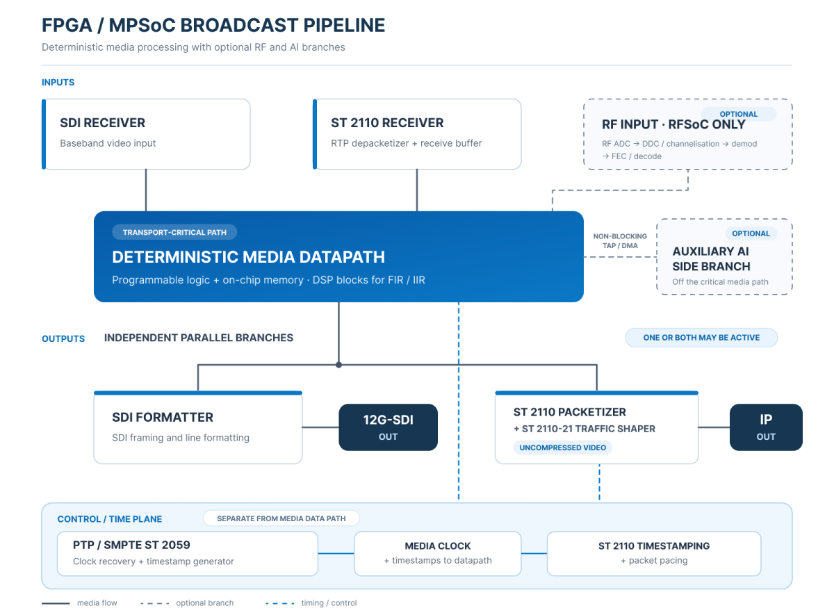
A contention problem stays quiet until a heavier concurrent load starves shared memory access for a few microseconds — long enough to underrun a channel buffer, short enough that a single-path bench never triggers it. How to isolate any side branch and where to place buffers is therefore an architecture decision made early. Synchronization is just as quiet: ST 2110 sits on PTP under the SMPTE ST 2059 profile, but a working facility needs the whole timing-and-control stack around it, and a device has to ride out a brief PTP disruption and recover cleanly. The EBU frames exactly this surrounding stack in its Technology Pyramid for Media Nodes (EBU Tech 3371) — ST 2110 is only the tip; timing, discovery, and control are where deployments actually break.
Failure Patterns
The figures below illustrate the mechanism; they are not measured telemetry from a specific project.
Scenario 1 — contention at full count. Clean at a partial channel count on the bench; at full production count the datapath and side processing contend for interconnect and memory, and one or two channels underrun intermittently — never reproducibly, because the trigger is the exact concurrency the bench never ran.
Scenario 2 — margin on the real board. Latency holds at startup, then degrades as the enclosure heats and a system-level thermal policy reduces a clock. Crossing FIFOs sized for the nominal clock begin to back-pressure, and ST 2110-21 shaping on the uncompressed-video flow slips — a fault that only appears on the production board under thermal soak, not on the eval kit.
Scenario 3 — PTP recovery. Single-stream validation passes. After a network disruption, PTP recovers more slowly than the budget assumed, and for that window the packetizer timestamps against a drifting clock. Audio, at finer sample timing, often shows it first — but PTP is the first subsystem to check, not the only one: RTP timestamp discontinuity, buffer management, and sample-rate conversion can produce the same symptom.
FPGA and MPSoC Pipeline Engineering
Engineering Experience Across FPGA, MPSoC, and Broadcast Platforms






A Single-Chip SDI and ST 2110 Broadcast Platform on One Zynq UltraScale+ MPSoC
For SONOVTS Media GmbH — the German broadcast specialist behind the HDQLINE professional UHD/4K display platform — Promwad designed a hardware platform intended to support both SDI and ST 2110 from the board's core, replacing a two-chip design (a separate TI Sitara processor plus a Kintex UltraScale+ FPGA) with a single AMD Zynq UltraScale+ MPSoC. The board carries two 12G-SDI inputs, HDMI/DisplayPort, Gigabit Ethernet, USB, and panel outputs, with the FPGA's high-speed transceivers carrying the ST 2110 transport-layer data path, on a power tree redesigned around the new SoC. This is an MPSoC platform, not an RFSoC-plus-AI design — the clearest public example of putting SDI capture and ST 2110 transport on one device: the Zynq UltraScale+ SDI/ST 2110 hardware platform. Hardware design was Promwad's scope; the client kept FPGA firmware, board bring-up, and manufacturing in-house.
Solution Approach
Step 1 — Map the clock domains and crossings. Document every clock domain and crossing before touching datapath logic. Verify synchronizer correctness (latent defects) and size crossing FIFOs against worst-case channel count and burst (throughput defects), and confirm behavior if a thermal policy reduces a clock.
Step 2 — Measure contention, and validate the real board. Instrument interconnect and memory under concurrent load on target silicon, capturing sustained (not peak) usage per path; then validate the production board itself — clock jitter, SI/PI, DDR calibration, transceiver eye, and thermal soak. Both belong in a SoC/MPSoC architecture review, before architecture/RTL freeze and PCB design release.
Step 3 — Keep the datapath deterministic. Assign essence functions to a deterministic FPGA datapath (FIR/IIR on DSP blocks; routing, buffering, and packetization in programmable logic and on-chip memory), keep any AI on a non-blocking side branch, and validate ST 2110-21 shaping on the uncompressed-video flow and PTP recovery under sustained load.
An eval-board number is a best-case baseline. The pipeline's real timing is set by what happens when the datapath and the rest of the system contend for interconnect and memory — on the production board, under sustained multi-channel load, across a real thermal range.
Real Trade-Offs
Choosing the platform class. SDI/ST 2110 without direct-RF → a general FPGA or MPSoC; a design that needs integrated RF ADC/DAC (an RF-enabled contribution gateway, modem, or wireless link) → Zynq UltraScale+ RFSoC; extreme RF bandwidth plus hardened DSP → evaluate AMD's Versal RF against availability, price, and lifecycle.
Zynq UltraScale+ RFSoC vs Versal RF. AMD announced the Versal RF Series on 10 December 2024 as its 5th-generation direct-RF family (hardened DSP plus AI Engines, up to ~80 TOPS of DSP compute), positioned mainly for aerospace, defense, and test & measurement; engineering samples began shipping in late 2025, with production shipments expected in H1 2027. For broadcast programs without those extreme-RF needs, Zynq UltraScale+ RFSoC remains the proven, available base.
FPGA inline processing vs host/GPU with NIC-assisted transport. Both can deliver hardware-assisted packet pacing. An FPGA gives tightly integrated inline processing, custom I/O, and a fixed pipeline; a host/GPU pipeline with a NIC such as NVIDIA Rivermax — which does hardware pacing on the NIC and supports ST 2110-21 — gives COTS scalability, GPU-direct processing, and software-defined deployment. The trade is integration and determinism-by-design vs commodity scale, examined across broadcast technology solutions.
Qualifying Symptoms
You may be facing this if:
- The design meets its targets on the bench but loses them as a full multi-channel media chain on the production board.
- Channel underruns appear only at full channel count and never reproduce on the bench.
- Timing holds at startup, then degrades once the enclosure heats and a thermal policy reduces a clock.
- Sync problems appear only after a network event, reboot, or wake — PTP recovery is slower than the budget assumed.
- Receivers on the ST 2110 side lose packets while the datapath reports clean — worth checking shaping (2110-21) and the network, not just the device.
At this point the work is clocking, contention, and board-level analysis, not a faster device: map clock domains and crossings, measure contention under concurrent load, validate the production board's margins, and confirm PTP recovery and ST 2110-21 shaping under sustained load. That work sits in FPGA & SoC design, with the deterministic media layer in FPGA-based video and audio processing and ST 2110 / NMOS integration. The deterministic-DSP foundation these pipelines build on is covered in FPGA-based audio processing for broadcasting and telecom.
FAQ
Why does my design meet its numbers on the bench but miss them in production?
Do most broadcast designs even need RFSoC?
Can I put an AI model in the real-time path?
Audio drifts after a network event while video is fine — is it PTP?
Related Engineering Cases
- SDI + ST 2110 on one MPSoC — Zynq UltraScale+ SDI/ST 2110 hardware platform (SONOVTS). Single-device SDI capture and ST 2110 transport; hardware scope.
- FPGA SDI-to-IP under multi-stream load — High-speed OpenGear cards for multi-camera broadcasting.
- SDI link-format conversion in the FPGA datapath — 3G/12G SDI gearbox (4×3G↔12G, 2SI/SQD), a micro-case in the SoC/MPSoC projects review.
- RFSoC data capture and clocking (adjacent RF competency, not a broadcast case) — RFSoC ADC data capture: gapless PL→PS transfer with clocking-subsystem configuration over I2C/SPI.
These public references cover adjacent parts of the architecture; they are not presented as one combined RFSoC + AI + ST 2110 project.