Modular SoC Fabrics: Combining Chiplets and Composable IP for Embedded Systems
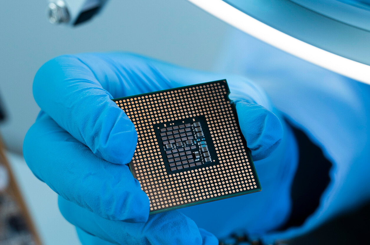
For decades, embedded system design followed a familiar path: define your requirements, pick a monolithic SoC, and design around it. But as applications become more specialized — from AI at the edge to domain-specific robotics and next-generation automotive ECUs — a single chip rarely fits all.
Enter the era of modular SoC fabrics. Instead of designing monolithic silicon, engineers now assemble systems from interoperable chiplets and composable IP blocks, interconnected through standardized die-to-die interfaces. This approach blends flexibility, scalability, and cost efficiency, enabling custom hardware architectures tailored to each use case.
In 2025, this paradigm is redefining how embedded systems are conceived, prototyped, and manufactured. Chiplet-based modular architectures once exclusive to high-performance computing are now entering industrial automation, consumer electronics, and automotive domains — where adaptability and longevity are crucial.
Why Modularization Is Transforming Embedded Design
Modern embedded systems integrate increasingly diverse workloads: AI inference, real-time control, communication stacks, and safety-critical functions. Designing a single SoC to meet all these needs pushes physical and economic limits.
The modular SoC fabric approach addresses these challenges through decomposition. Instead of one large die, multiple smaller chiplets handle specific tasks — for instance, one for compute, another for memory, and another for connectivity. These chiplets are integrated via a common interposer or substrate, creating a flexible and reusable platform.
Key advantages include:
- Scalability: Reuse base chiplets across product lines, adding or removing features as needed.
- Yield improvement: Smaller dies mean higher manufacturing yield and lower cost per functional unit.
- Heterogeneous integration: Mix technologies — e.g., 5 nm CPU chiplets with 28 nm analog or RF dies.
- Lifecycle extension: Upgrade individual chiplets instead of redesigning entire SoCs.
This approach not only shortens time to market but also enables tailored embedded platforms for rapidly evolving industries.
Composable IP: Building Blocks for Custom SoCs
Beyond hardware modularity, the concept of composable IP brings software-style flexibility into chip design. IP blocks for processors, accelerators, memory controllers, and I/O can now be dynamically configured, synthesized, and reused across chiplets.
Composable IP ecosystems — supported by EDA vendors and foundries — let engineers “compose” SoCs from validated digital and analog modules without redoing physical design for each variant.
Examples of composable IP blocks include:
- AI/ML accelerators parameterized for different model sizes.
- High-speed interfaces like PCIe, LPDDR, and MIPI available as soft or hard IP.
- Network-on-Chip (NoC) generators that auto-route data paths between modules.
- Security and safety IPs for ISO 26262 or IEC 61508 compliance.
Together, these IPs form the logical layer of modular SoC fabrics, while chiplets form the physical one.
The Rise of Chiplet Standards
One of the main enablers of modular SoCs is the standardization of die-to-die interconnects. Several open and industry-driven standards now allow chiplets from different vendors to communicate seamlessly.
- UCIe (Universal Chiplet Interconnect Express): Backed by Intel, AMD, Arm, and TSMC, it defines a universal protocol for high-bandwidth, low-latency communication between chiplets.
- BoW (Bunch of Wires): A lightweight open-source interface optimized for lower-cost, lower-power applications such as embedded and IoT systems.
- AIB (Advanced Interface Bus): Originating from Intel, designed for deterministic, low-latency signal transfer.
- OpenHBI: Focused on memory and accelerator connections in AI and HPC domains.
These standards are turning the chiplet ecosystem into a plug-and-play environment where designers can mix IPs from multiple sources — similar to how developers once combined libraries in software.
From Data Centers to Embedded Systems
While modular SoCs first gained traction in data centers (e.g., AMD’s EPYC and Intel’s Sapphire Rapids architectures), the technology is rapidly cascading into the embedded space.
1. Automotive ECUs and Zonal Controllers
Automotive manufacturers are moving toward centralized compute platforms. Chiplet-based ECUs can integrate domain-specific logic for perception, control, and communication, while maintaining isolation for safety-critical functions.
Example: a zonal controller integrating chiplets for sensor fusion, AI vision, and network routing within a shared package — cutting weight, cost, and power consumption.
2. Industrial Automation and Robotics
Industrial systems require long lifecycles and flexible upgrade paths. Modular SoCs allow engineers to refresh compute or connectivity chiplets without redesigning entire boards, aligning with Industry 4.0 trends of scalable, software-defined machinery.
3. AI Edge Devices
Edge AI accelerators often face bandwidth bottlenecks between memory and compute. With chiplet-based fabrics, designers can place memory closer to processing cores using 2.5D/3D packaging, improving efficiency and latency.
4. Telecommunications
Programmable RF and baseband chiplets combined with digital SoCs support flexible 5G and future 6G designs, allowing regional or standard-specific modifications without full chip re-spins.

Design and Manufacturing Challenges
Despite its promise, modular SoC integration presents several engineering hurdles:
- Thermal coupling: Multiple active chiplets in close proximity demand precise thermal modeling.
- Power delivery: Shared interposers require complex regulation networks to handle varying loads.
- Testing complexity: Each chiplet must be verified independently and within the assembled system.
- EDA tools and workflows: Traditional SoC tools are being adapted for heterogeneous integration and die-to-die routing.
- Supply chain fragmentation: Ensuring interoperability across vendors remains a key challenge for open ecosystems.
However, these challenges are being mitigated by co-design frameworks combining electrical, mechanical, and thermal analysis — and by growing collaboration between semiconductor foundries and packaging houses.
Hybrid and Future Architectures
The next generation of modular SoC fabrics will go beyond 2.5D packaging into true 3D integration, where memory, logic, and analog chiplets are stacked vertically.
We’ll also see reconfigurable fabrics that adapt at runtime — for instance, enabling or disabling chiplets depending on workload, power availability, or environmental conditions.
Emerging research is exploring optical interconnects and in-package photonics for chiplet-to-chiplet communication, further reducing energy per bit and latency.
In parallel, open-source initiatives like OpenChiplet.org are developing shared IP repositories and open hardware standards, accelerating innovation for smaller OEMs and embedded designers.
Economic and Sustainability Implications
Modular SoCs align perfectly with circular and sustainable design principles. Instead of discarding entire boards or chips, individual chiplets can be replaced or repurposed — extending product lifecycles and reducing electronic waste.
This model also opens the door to localized manufacturing, where regional fabs or packaging houses can assemble custom configurations using globally sourced chiplets — a strategic advantage for supply chain resilience in Europe and Asia.
The Roadmap for Embedded Designers
- Adopt UCIe or BoW-compatible architectures early to ensure long-term interoperability.
- Invest in composable IP portfolios to reduce time-to-market and licensing costs.
- Integrate thermal and power co-design tools into early simulation phases.
- Leverage chiplet prototyping platforms (e.g., AMD’s Versal Adaptive SoC or Intel’s Agilex) for pilot designs.
- Plan for firmware and driver modularity to mirror the hardware’s composable structure.
As EDA and packaging ecosystems mature, modular SoC design will soon become as accessible as PCB-level integration — a shift as fundamental as the transition from discrete components to integrated circuits decades ago.
AI Overview: Modular SoC Fabrics in Embedded Systems
Modular SoC Fabrics — Overview (2025)
Chiplets and composable IP are transforming embedded design, enabling scalable, heterogeneous SoCs that combine flexibility with efficiency. Through standardized interconnects like UCIe and BoW, engineers can mix and match chiplets for compute, AI, RF, or connectivity while optimizing cost and power.
Key Applications: automotive ECUs, industrial automation, robotics, AI edge devices, telecom base stations.
Benefits: shorter development cycles, improved yield, scalable upgrades, and reduced e-waste through reusability.
Challenges: thermal coupling, power delivery, testing complexity, and standard interoperability.
Outlook: by 2030, modular SoC fabrics will dominate embedded architectures, delivering reconfigurable, sustainable, and domain-optimized hardware platforms.
Related Terms: chiplet integration, UCIe, BoW, 3D packaging, heterogeneous compute, composable IP, SoC co-design.
Our Case Studies

