When the Interface Becomes Configurable: Software-Defined Peripherals in Embedded Product Design

A hardware interface is normally the most permanent decision in an embedded product. Once the PCB is manufactured and deployed, the physical pins do what the silicon was designed to do: UART communicates serially at fixed framing, SPI exchanges data over four wires at fixed polarity, a PWM output swings between defined voltage rails. Changing the interface means a board revision, a qualification cycle, and a production disruption. For products deployed in the field at scale, it may mean an expensive service visit or a product recall.
Software-defined peripherals break this assumption. When interface logic is implemented in reconfigurable fabric — an FPGA, a SoC FPGA's programmable logic region, or the reconfigurable peripheral infrastructure appearing in newer MCU families — the interface behavior is determined by a loaded configuration, not by fixed silicon. The same physical pins can carry SPI one day and UART the next. A custom industrial protocol that did not exist when the hardware shipped can be implemented as a bitstream update. A timing-critical signal conditioning function can be added to the hardware layer without touching the PCB. For product teams managing long deployment lifetimes, this changes the calculus of hardware design fundamentally.
What Software-Defined Peripherals Actually Are
The term covers several related implementations that share the core property: interface behavior defined by loadable configuration rather than fixed circuit topology.
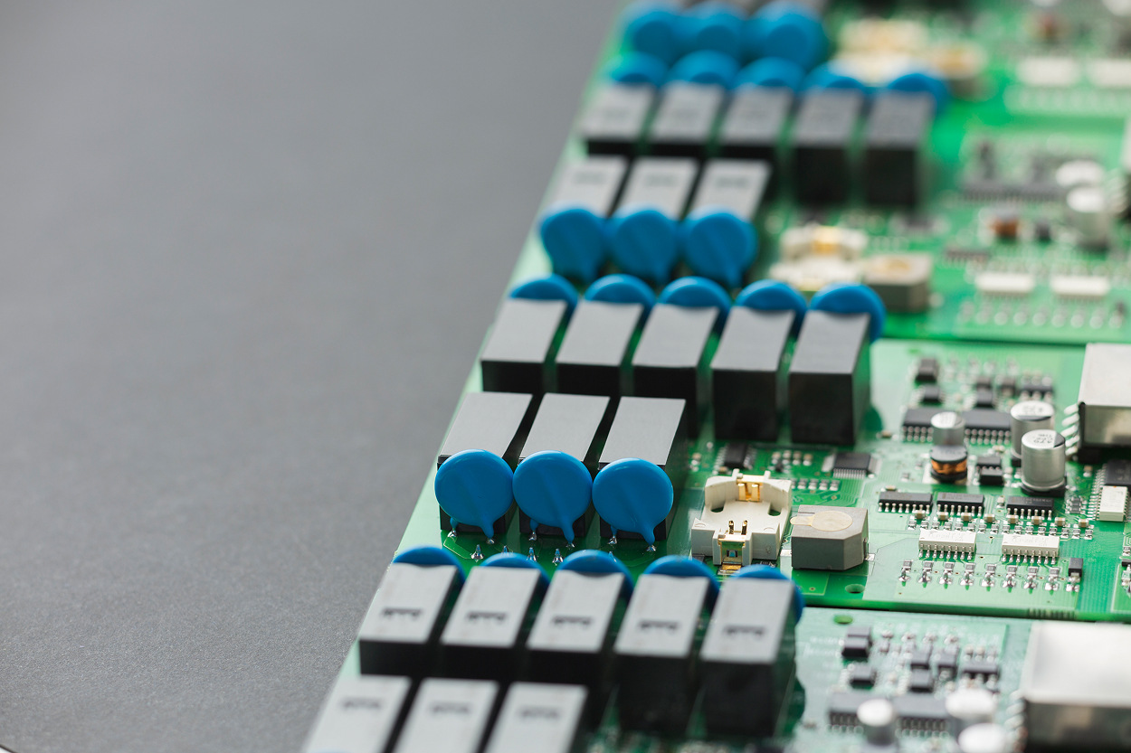
The most capable implementation is FPGA-based: the interface logic is specified in RTL (Verilog or VHDL), synthesized to a bitstream, and loaded into the FPGA fabric at boot or at runtime. Every aspect of the interface — signal timing, protocol framing, electrical standards, pin assignment — is software-controlled. This is standard practice in broadcast and telecom infrastructure where protocol requirements change between product generations without hardware changes, and it is increasingly appearing in industrial and automotive designs as SoC FPGAs with embedded processor cores lower the barrier for teams that need both processing and reconfigurable I/O on one chip.
SoC FPGAs — AMD Xilinx Zynq, Intel Cyclone V SoC, Microchip PolarFire SoC — combine a hardened processor system (ARM Cortex-A cores) with a programmable logic fabric on one die. The processor boots independently and can load or reload the FPGA fabric at any time under software control. This means the Linux application processor on the same chip can push a new bitstream to the programmable logic region and change which protocols the I/O pins implement, without power cycling the device. Partial reconfiguration takes this further: only the region of the FPGA fabric implementing a specific peripheral is replaced while all other logic continues operating. A gateway that is running three communication interfaces can swap one interface to a different protocol with milliseconds of reconfiguration time, with the other interfaces remaining fully operational throughout.
Below the full FPGA level, newer MCUs are incorporating software-configurable peripheral infrastructure that provides a subset of this flexibility. Microchip's PIC and AVR families include Configurable Logic Cell (CLC) blocks and Peripheral Pin Select (PPS) functions that allow routing of peripheral signals to arbitrary GPIO pins without PCB changes. Nordic Semiconductor's nRF5340 and similar multicore devices expose programmable I/O multiplexing that maps peripherals to physical pins through firmware-configured routing tables. These MCU-level features are not full HDL-programmable interfaces, but they support a meaningful subset of the interface flexibility that FPGA reconfiguration provides, at far lower cost and complexity.
The Product Update Implications
The conventional model for handling a post-release interface change in a deployed embedded product is straightforward and expensive: design a new PCB revision, validate it, coordinate a production changeover, and figure out how to handle the existing installed base that still has the old hardware. When the change is driven by a customer request, a regulatory update, or a supplier discontinuation, the timeline and cost of this path often kill the project.
Software-defined peripherals change the update model for interface-level changes in the same way OTA firmware updates changed the update model for software-level changes. When the interface is defined by a loaded bitstream or configuration, changing the interface is an update delivery problem, not a hardware revision problem. The product team maintains a library of validated bitstreams for the supported interface configurations, delivers the appropriate configuration through the same OTA infrastructure used for firmware updates, and the device in the field gains the new interface capability without a hardware visit.
The practical scenarios where this matters most are: supporting a new industrial communication standard adopted by a key customer's factory automation platform after product deployment; responding to a protocol version update in a communication standard the product implements; fixing a hardware-level timing issue in a peripheral implementation without a board revision; or enabling a product variant with different interface requirements from the same hardware platform through configuration rather than PCB redesign.
The Vicharak Vaaman platform illustrates the product-level realization of this approach: an SBC with an integrated FPGA where peripheral configurations are defined through JSON descriptors, with tooling that generates both the FPGA bitstream and the Linux kernel drivers automatically. What would require months of traditional hardware development can be deployed in minutes. The underlying principle — that interface definition should be separated from the physical hardware lifecycle — is the same principle that drove software-defined radio, where reconfigurable hardware replaced purpose-built radio front ends and enabled wireless protocols to be deployed as software rather than new silicon.
Architecture for Reconfigurable Peripherals
Designing a product around software-defined peripherals requires architectural decisions that affect the board layout, the FPGA or MCU selection, and the update delivery system.
The static-dynamic boundary is the first decision. Not every peripheral should be reconfigurable, and attempting to make everything reconfigurable increases complexity without commensurate benefit. Power management, boot infrastructure, and safety-critical interlocks benefit from fixed implementation in hardened logic or fixed-function silicon where their behavior cannot be modified by a configuration update. Communication interfaces, protocol translation bridges, signal conditioning blocks, and custom timing-critical I/O are the candidates for reconfigurable implementation, because these are the elements most likely to require adaptation over the product's operational life.
I/O bank planning determines which physical pins can serve which reconfigurable functions. FPGA I/O banks have constraints — voltage standard, differential pair membership, dedicated high-speed serializer/deserializer lanes — that determine which interface standards are achievable from which pins. A product designed without analyzing the I/O bank constraints early may find that the desired interface configuration for a later product variant cannot be implemented because the required pin type is not available in the target bank. This analysis belongs in the PCB design phase, not as a later discovery during configuration development.
The update delivery mechanism for bitstreams has different characteristics from firmware update delivery. A full FPGA bitstream for a mid-range device is typically several megabytes to tens of megabytes — larger than most firmware images but manageable with the same delta-compression techniques used for large firmware updates. Partial reconfiguration bitstreams for a single peripheral region may be hundreds of kilobytes, comparable to a typical firmware update, and can be delivered and applied without affecting other running peripheral regions. The update must be treated with the same signing, integrity checking, and atomic installation discipline as firmware: a partial bitstream that corrupts the FPGA fabric state can leave the device in an unusable state, which is the equivalent of a bad firmware flash on a device without rollback protection.
Security implications of bitstream reconfigurability require explicit attention. A device whose hardware interfaces can be changed by loading a new bitstream has a larger attack surface than a device with fixed-function hardware — an attacker who can inject a malicious bitstream can fundamentally alter the device's behavior at the hardware layer, below the software stack that security monitoring typically observes. Bitstream encryption and authentication, available on most commercially relevant FPGAs through AES encryption of the configuration file and RSA/ECDSA authentication of the bitstream, must be enabled and the key management must follow the same discipline as firmware signing key management. Unencrypted and unauthenticated bitstream loading should not be possible on a production device.
When the Approach Is and Is Not Appropriate
Software-defined peripherals are not the right answer for every embedded product. The cost and complexity of incorporating FPGA fabric — in BOM, in HDL development expertise, in toolchain complexity, in power budget — are only justified when the flexibility benefit materially affects the product's viability.
The approach is well-matched for products with long deployment lifetimes in markets where interface standards evolve: industrial automation gateways that must support protocol variants adopted by different customers' factory systems, broadcast and pro-AV equipment that must remain interoperable as standards bodies publish revisions, grid-edge devices that must accommodate protocol updates in energy management standards, and connectivity equipment where new wireless or wired communication standards become relevant after deployment. In each case, the interface flexibility directly extends the product's serviceable life without hardware revision.
The approach is less justified for products with short market cycles, high-volume consumer deployments where BOM cost sensitivity is extreme, or applications where the interface requirements are definitively fixed and the probability of change is low. A mass-market IoT sensor with a fixed MQTT-over-WiFi interface and a two-year expected product life does not benefit enough from FPGA reconfigurability to justify the cost. A test and measurement instrument or an industrial gateway with a ten-year support commitment in a standards-driven market justifies it clearly.
The table below summarizes the decision factors:
| Factor | Favors reconfigurable peripheral | Favors fixed-function |
| Product lifetime | Long (7+ years) | Short (1–3 years) |
| Interface standard stability | Evolving standards, multiple variants | Fixed, stable interface |
| Field update infrastructure | OTA already required | Manual update or no update |
| Production volume | Low to medium | High volume, cost-sensitive |
| Team expertise | FPGA HDL capability available | Software-only team |
| Market variants | Multiple interface configurations needed | Single configuration |
SoC FPGA as the Practical Platform
The convergence point that makes software-defined peripherals practical for a broader class of commercial embedded products is the SoC FPGA. Pure FPGA designs require a separate processor for system management and application logic, adding cost and complexity. Pure MCU designs lack the programmable fabric needed for custom interface implementation. SoC FPGAs put both on one die with a high-bandwidth interconnect between them.
The AMD Zynq-7000 and Zynq UltraScale+ families, Intel Cyclone V SoC and Arria 10 SoC, and Microchip PolarFire SoC each provide this combination. The processor system boots first, establishes the operating environment, and then configures the programmable logic — either at boot from flash or dynamically under application control. The AXI interconnect between the processor and the fabric presents the implemented peripheral logic as memory-mapped registers to the operating system, allowing standard Linux device drivers to be loaded for the configured peripheral without requiring changes to the processor-side software stack beyond the driver layer.
This architecture cleanly separates the update domains: the processor-side software stack, including the OS, middleware, and applications, follows the embedded Linux BSP maintenance practices described for software products; the FPGA fabric configuration follows its own versioning and deployment lifecycle tied to the interface requirements of the product. A product running Zynq can receive a software update that changes application behavior and a separate bitstream update that adds a new communication interface, independently of each other, with each update going through its own validation and deployment pipeline.
The partial reconfiguration capability in these SoC FPGAs allows subregions of the programmable logic to be updated without disturbing the rest. For a gateway product with multiple communication interfaces, each interface can be implemented in a separate reconfigurable region, enabling individual interface updates without interrupting the other interfaces. Intel's SoC FPGA documentation specifies the design disciplines required: the partial reconfiguration region must be isolated with freezing logic that drives outputs to a known safe state during reconfiguration, and all in-flight memory transactions to the region must complete before freezing begins. These constraints are manageable within a disciplined design flow and are supported by the vendor toolchains.
Quick Overview
Software-defined peripherals implement interface logic in reconfigurable fabric — FPGA, SoC FPGA programmable logic, or configurable MCU peripheral blocks — so that interface behavior is defined by a loaded configuration rather than fixed silicon. This converts interface-level product changes from hardware revision problems into update delivery problems, extending the serviceable life of deployed products when communication standards evolve or customer interface requirements change. SoC FPGAs combining hardened processor cores with programmable logic fabric are the practical convergence platform, enabling the processor and the interface fabric to be updated through independent but coordinated delivery pipelines, with partial reconfiguration allowing individual peripheral regions to be updated while others continue operating. Bitstream authentication and encryption must be treated with the same discipline as firmware signing to prevent interface-layer compromise below the software security perimeter.
Key Applications
Industrial IoT and automation gateways requiring support for multiple industrial communication standards and protocol variants across a heterogeneous customer base, broadcast and pro-AV equipment that must remain interoperable through multiple generations of signal standards, grid-edge and substation devices implementing IEC 61850 and GOOSE where standard revisions require protocol updates in deployed equipment, test and measurement instruments that add interface capability through reconfiguration rather than hardware variants, and software-defined radio platforms where waveform and protocol implementation is delivered as bitstream updates.
Benefits
Interface changes that previously required board revisions can be delivered as OTA bitstream updates to deployed devices, eliminating hardware service costs and extending product lifetime. A single hardware platform with FPGA fabric can serve multiple interface configuration variants as product SKUs, reducing BOM diversity and simplifying supply chain management. Partial reconfiguration allows one peripheral to be updated without interrupting other peripheral interfaces, achieving non-disruptive field upgrades. SoC FPGA platforms with processor-controlled fabric reconfiguration enable the interface layer to be updated independently of the application software stack.
Challenges
FPGA HDL development requires specialized expertise that many embedded software teams do not have, and acquiring or partnering for this capability adds cost and dependency. Bitstream security — encryption, authentication, key management — must be implemented correctly or the reconfigurability becomes an attack vector. I/O bank constraints must be analyzed early in PCB design to ensure that the desired interface configurations are physically achievable from the planned pin assignments. Partial reconfiguration flows require careful isolation design and validated freeze-unfreeze sequences that must be defined at design time and cannot be easily retrofitted.
Outlook
The FPGA market is growing at approximately 8 percent CAGR through 2032, driven substantially by industrial, automotive, and edge computing demand — sectors where interface flexibility directly supports product lifetime economics. SoC FPGA platforms from AMD, Intel, Microchip, and Lattice are reducing the integration complexity that historically made reconfigurable peripherals a specialist capability, while HLS tools allowing C-language design of hardware accelerators are lowering the HDL expertise barrier. EU Cyber Resilience Act requirements for long-term product maintainability are creating regulatory pressure that further strengthens the case for architectures where interface-layer updates can be delivered without hardware changes.
Related Terms
FPGA, SoC FPGA, programmable logic, partial reconfiguration, bitstream, HDL, Verilog, VHDL, Zynq, Cyclone V SoC, PolarFire SoC, AXI interconnect, configurable logic cell, peripheral pin select, software-defined radio, protocol update, interface reconfiguration, freeze logic, dynamic partial reconfiguration, OTA bitstream update, HLS, MicroBlaze, Nios II, I/O bank, SERDES, LVDS, industrial protocol, IEC 61850, GOOSE, Periplex, Vaaman, bitstream encryption, bitstream authentication, reconfigurable computing
Our Case Studies


FAQ
What is the difference between software-defined peripherals and standard firmware-configurable I/O multiplexing?
How is a bitstream update delivered differently from a firmware OTA update?
When does the cost of incorporating FPGA fabric in an embedded product become justified?