
High-Speed
PCB Design
High-Speed PCB Design
High-speed PCB manufacturing and design at Promwad are focused on producing printed circuit boards capable of handling rapid signal transmission and minimising signal integity issues. Employ our expertise in multi-layer, mixed-signal, and high-speed board design services from the block diagrams to all necessary documentation and manufacturing support.
Besides high-speed designs, we obtain full-fledged capabilities for hardware simulation & analysis: pre-layout and post-layout signal integrity, power integrity, thermal analysis, and EMC/EMI. Our advanced tools and experienced engineers ensure the seamless design and optimisation of high-performance electronic systems.
Design Procedure
Each project comprise a diverse set of offerings and services, but the overall high-speed PCB manufacturing procedure consists of:
![]() Block diagram
Block diagram
![]() Design specification
Design specification
![]() Library components review
Library components review
![]() Schematic design
Schematic design
![]() Schematic review FW engineer
Schematic review FW engineer
![]() Components placement
Components placement
![]() Layer stack calculation
Layer stack calculation
![]() Pre-layout analysis
Pre-layout analysis
![]() PCB routing
PCB routing
![]() PCB layout review
PCB layout review
![]() Post-layout analysis
Post-layout analysis
![]() Design documentation development
Design documentation development
Result: We take responsibility for each stage of the PCB manufacturing process, as well including handling challenges like reduced engineering time or increased complexity. We make sure you get the best quality design on time and budget.


Our Experience
PCIe – 6; FMC cards – 12; PCIe104 – 3; PXIe – 1; SoM – 7; RF – 3; mini-PCIe – 2
PCIe, 10GbE, 100GbE; CameraLink, MIPI, HDMI, DP; DDR4, JESD204b
Featured Case Study
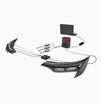
Satellite modem design
We designed the device in a compact 1U form factor by dividing it into digital and analog boards. Our engineers have developed a dedicated front end using high-speed ADC/DAC converters and modern high-frequency analog modulators/demodulators. We reached high-speed data exchange between server and device with the help of four 10G interfaces and the DPDK framework. To configure the device and measure the signal parameters, we developed a graphic application.
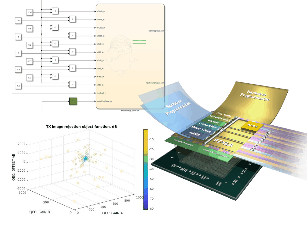
Hardware Simulation and Analysis
We deliver high-speed PCB manufacturing solutions along with combined signal integrity, power integrity, thermal analysis, and EMI/EMC.
Design Output Options
By request of our customers, we provide preferable for them design documentation options:
PCB Manufacturing
- Gerber and NC drill files
- ODB++ (if needed)
- IPC-D-356 file for electrical test
- Drill drawing PDF-file
Assembly Manufacturing
- BOM
- Stensil apertures for solder paste
- Component placement file
- Assembly diagram for top and bottom layers
- Shematic files
Our Hardware Development Projects
As a hardware development company, we have successfully completed numerous projects for a diverse range of industries, including telecommunications, automotive, and consumer electronics.


Do you need a quote for a high-speed PCB design project?
Please, drop us a line. We will contact you today or next business day. All submitted information will be kept confidential.