32 GT/s on the Board: What PCIe Gen 5 Actually Changes for Embedded System Designers
PCIe bandwidth has doubled with every generation since the standard's introduction, and each doubling has been accompanied by a proportional increase in the difficulty of the board-level signal integrity work required to make it function reliably. PCIe Gen 5 at 32 GT/s pushes the Nyquist frequency of the NRZ signal to 16 GHz — precisely where the physics of standard PCB dielectric and trace geometry impose losses that consume nearly the entire insertion loss budget before the signal reaches the receiver. The 36 dB total insertion loss budget that PCIe Gen 5 specifies is not generous: it leaves system designers with approximately 16 dB for the PCB trace on the system baseboard before accounting for connectors, vias, component packages, and any cable segments.
For server platform designers working with Intel Sapphire Rapids, AMD EPYC Genoa/Turin, or ARM Neoverse platforms that expose 128+ PCIe 5.0 lanes, these challenges are addressed by teams with deep signal integrity expertise and access to high-volume PCB qualification infrastructure. For embedded compute designers integrating PCIe 5.0 on industrial SBCs, GPU attach boards, AI inference accelerator platforms, or edge compute modules, the same physics apply with narrower engineering margins, smaller PCB formats, tighter thermal constraints, and less budget for the high-speed PCB materials and retimer ICs that make the difference between a functional PCIe 5.0 link and one that trains at Gen 3.
This article addresses what PCIe Gen 5 changes specifically for three embedded application categories — NVMe storage, GPU attach, and AI accelerators — and what the board design implications are for each.
What PCIe Gen 5 Is — and What It Is Not
PCIe Gen 5 doubles per-lane bandwidth from PCIe Gen 4's 16 GT/s to 32 GT/s, using the same 128b/130b encoding and NRZ signaling that Gen 4 uses. An x16 PCIe Gen 5 slot delivers approximately 63 GB/s of bidirectional bandwidth — twice Gen 4's 32 GB/s. This is the number that makes PCIe Gen 5 relevant for feeding data-hungry AI accelerators, loading LLM checkpoints into GPU VRAM, and sustaining the throughput that Gen 5 NVMe SSDs can deliver at 14–14.5 GB/s sequential read.
PCIe Gen 5 is not PAM4. PAM4 is PCIe Gen 6's encoding scheme. Gen 5 stays with NRZ, which means the full bit rate arrives at the Nyquist frequency as a sinusoidal fundamental component — the 16 GHz sine wave for 32 GT/s NRZ. This single decision — NRZ rather than PAM4 — is both the blessing and the curse of PCIe Gen 5 for board designers. NRZ at 16 GHz Nyquist is familiar in its structure (same equalizer architecture as Gen 4, same 128b/130b coding, same BER requirement of 10−12) but demanding in its loss budget. An 800 mV p-p NRZ signal at the transmitter attenuates to approximately 12.7 mV after 36 dB of channel insertion loss — leaving a tiny residual signal for the receiver's equalizer to work with. The PCIe Gen 5 receiver's equalization chain is correspondingly more capable than Gen 4: the continuous-time linear equalizer (CTLE) has ADC down to −15 dB (versus −12 dB for Gen 4), and the decision feedback equalizer (DFE) has three taps (versus two for Gen 4).
Backward compatibility is preserved: PCIe Gen 5 slots accept Gen 4, Gen 3, and earlier cards, and Gen 5 devices negotiate down to Gen 4 on platforms that only support Gen 4. The physical connector is mechanically compatible with prior CEM specifications. The entire protocol layer — transaction layer, data link layer, physical layer coding — is otherwise unchanged from Gen 4.
The Signal Integrity Problem and How It Is Solved
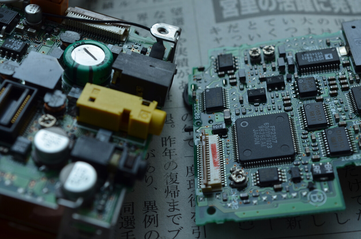
The insertion loss budget for PCIe Gen 5 from chip bump to chip bump is 36 dB. In a typical system configuration on a standard PCB material (FR4, loss tangent around 0.02), a 1-inch trace at 16 GHz loses approximately 1.5–2 dB/inch depending on trace geometry. A 10-inch routing path — realistic for a CPU-to-PCIe slot routing on a full-ATX or even a compact embedded carrier board — consumes 15–20 dB of the budget in PCB trace alone, before the via transitions, BGA package escapes, edge connector, and the add-in card's own trace are included.
At 16 GHz, small deviations that were tolerable at lower PCIe generations become board-level failure mechanisms. A nominally correct layout can still fail after fabrication if the real stackup shifts impedance, changes dielectric loss, or moves a via stub resonance into the operating band. This is why signal integrity at PCIe Gen 5 Nyquist frequencies has to be validated against fabrication tolerances before tape-out, not only during lab bring-up.
Three mitigation strategies, used in combination, address this:
PCB material upgrade: low-loss dielectrics — Panasonic Megtron 6, Rogers materials — reduce the loss tangent from FR4's 0.02 to approximately 0.004–0.007, cutting dielectric attenuation by 60–70 percent at 16 GHz. Texas Instruments' PCIe Gen 5 layout application note recommends Megtron 6 as the material of choice for Gen 5 designs. The cost premium over FR4 is significant — approximately 2–4× for the PCB itself — which is relevant for cost-sensitive embedded products.
Trace length minimization: keeping the CPU-to-slot routing as short as physically possible reduces the absolute insertion loss in proportion. This directly drives placement decisions: on embedded carrier boards designed for PCIe Gen 5, the M.2 key M slot or PCIe edge connector must be placed as close to the SoC BGA as the thermal management and component placement constraints allow.
Retimers: a PCIe Gen 5 retimer is an active component inserted in the middle of a PCIe lane that recovers the incoming signal — retiming, re-amplifying, and retransmitting a clean signal with the jitter and insertion loss budget reset. Unlike a passive redriver that amplifies both signal and noise, a retimer participates in the PCIe protocol (it terminates the link and establishes a new link segment), allowing the downstream segment to start from a full fresh budget. Texas Instruments' DS320PR1601 is a 32 Gbps, 16-lane PCIe 5.0 CXL 2.0 linear redriver; Astera Labs' Scorpio and Aries product lines provide retimer and smart retimer solutions for PCIe Gen 5 reach extension in server and now embedded applications. A retimer adds approximately 8 ns of added latency, which is relevant for latency-sensitive applications but negligible for throughput-bound storage and AI inference loading.
The insertion loss budget arithmetic for PCIe Gen 5 in embedded designs has a specific implication: on compact carrier boards (Mini-ITX, 3.5-inch SBC, SMARC 2.1 module with carrier), PCIe Gen 5 without retimers is achievable only with premium PCB materials and very short routing. On carrier boards that expose the SoC's PCIe Gen 5 lanes to external connectors with cable paths (external GPU cage, external storage expansion), retimers are required regardless of PCB material quality.
NVMe Gen 5 Storage — What Actually Changes
PCIe Gen 5 NVMe SSDs deliver sequential read performance of up to 14.5 GB/s — compared to approximately 7.5 GB/s for PCIe Gen 4 NVMe. This is not primarily relevant for the embedded applications where an SSD serves as the boot device or stores configuration data; it is relevant for the embedded compute category where the SSD is the primary data ingest path feeding a GPU or AI accelerator.
The specific scenario where Gen 5 NVMe materially changes embedded AI performance is checkpoint loading and dataset streaming. A modern LLM inference deployment loads model weights from SSD to GPU VRAM at startup and between requests. A 100 GB model checkpoint loaded from PCIe Gen 4 NVMe at 7.5 GB/s takes approximately 13 seconds; from PCIe Gen 5 NVMe at 14.5 GB/s, it takes approximately 7 seconds. For GPU utilization in a multiple-model inference stack that cycles through different models, this 2× improvement in load time directly reduces GPU idle time.
NVIDIA's GPU Direct Storage (GDS, accessed through the cuFile API) further amplifies this benefit by enabling direct DMA from NVMe to GPU HBM memory, bypassing the CPU DRAM bounce buffer that would otherwise introduce additional memory copy latency and CPU overhead. Dell's PERC H975i RAID controller, tested with PCIe Gen 5 x16 host interface and GDS-enabled NVMe drives, delivered 52.5 GB/s maximum throughput per controller in storage-to-GPU path testing, enabling H100 GPUs to sustain higher utilization during data-intensive training workloads. For embedded AI inference platforms — not data center training rigs — the relevant metric is time-to-first-token when a new model must be loaded, and Gen 5 NVMe halves that time compared to Gen 4.
The NVMe Gen 5 SSD's M.2 form factor (M.2 2280, M.2 22110) is unchanged from Gen 4, and the M.2 Key M socket supports both Gen 4 and Gen 5 at the mechanical level. What changes is the electrical requirement on the carrier board: the M.2 socket's PCIe traces must support Gen 5 routing, which means the trace length from SoC to socket must be within budget (with or without a retimer), and the PCB stackup must support the higher frequency. Many carrier boards from 2022–2023 that mechanically accept M.2 2280 were designed for Gen 4 and will negotiate Gen 5 SSDs down to Gen 4 — functioning correctly but not delivering the Gen 5 bandwidth.
GPU Attach at PCIe Gen 5
An x16 PCIe Gen 4 link delivers approximately 16 GB/s in each direction. An x16 PCIe Gen 5 link delivers approximately 32 GB/s. Whether a GPU's performance benefits from the additional bandwidth depends on the GPU's memory system bandwidth relative to the host interconnect bandwidth.
NVIDIA's A100 has 2 TB/s of HBM2e memory bandwidth. Its PCIe variant (as opposed to the NVLink-connected version) uses a PCIe Gen 4 x16 interface at 16 GB/s host bandwidth. The H100 PCIe variant uses PCIe Gen 5 x16 at 32 GB/s. A GPU operating on a compute-bound workload — where the bottleneck is in the matrix multiply units, not in host data transfer — will not benefit measurably from doubling the PCIe bandwidth. A GPU operating on a memory-bandwidth-bound inference workload where weights are streamed from host DRAM or NVMe because they do not fit in VRAM will benefit directly from the doubled PCIe host bandwidth.
For embedded compute contexts — a GPU-attached edge inference server, a robotics perception compute node, an ADAS domain controller using a discrete GPU for surround-view processing — the GPU usually operates close to its memory bandwidth limit on real workloads rather than at the PCIe interface limit. PCIe Gen 5 matters most in embedded GPU configurations where the GPU has modest VRAM (less than 16 GB) and must frequently reload model weights from host storage, or where multiple GPUs share PCIe lanes through a PCIe switch and the aggregate bandwidth of all GPUs approaches the Gen 4 x16 limit.
A three-level architecture analysis clarifies where PCIe Gen 5 is necessary:
| Scenario | GPU VRAM | Model fits in VRAM? | PCIe bandwidth sensitivity | Gen 5 impact |
| Single GPU, small model (< VRAM) | 24 GB | Yes | Low — weights loaded once | Minimal |
| Single GPU, large model (> VRAM) | 24 GB | No — streaming required | High | Significant |
| Multi-GPU x8/x8 split on x16 slot | 2 × GPU | Depends | Medium — shared bandwidth | Moderate |
| GPU + NVMe storage competing | 16 GB | Partial | High — storage-to-GPU path | Significant |
AI Accelerator Cards at PCIe Gen 5
The AI PCIe accelerator card market has expanded rapidly, with PCIe Gen 5 x16 becoming the standard host interface for high-performance edge inference cards. The global AI Accelerator PCIe Card market was estimated at 4.94 billion dollars in 2025 and is projected to reach 13.14 billion dollars by 2032 at 15 percent CAGR.
Intel's Agilex 7 FPGA-based accelerator card (HiprAcc NCS280-I) implements PCIe Gen 5 x16 plus CXL host connectivity in a half-length full-height form factor, delivering the full 64 GB/s bidirectional bandwidth of Gen 5 x16. The PCIe Gen 5 interface is particularly valuable for FPGA accelerators that perform data streaming — processing large data volumes that originate in host memory or NVMe storage and writing results back. At x16 Gen 5, the DMA throughput between the FPGA and host memory can approach 50 GB/s sustained, which is only achievable on prior generations with x16 Gen 4 at 32 GB/s.
Axelera's Metis AIPU PCIe card targets computer vision inference at edge servers with 214 TOPS (single AIPU) to 856 TOPS (quad AIPU) performance. These accelerators are primarily bandwidth-limited on the data path between the camera capture pipeline or NVMe-stored video frames and the NPU's local SRAM, making the PCIe Gen 5 bandwidth from host directly relevant to throughput.
The key embedded software architecture change that PCIe Gen 5 enables for AI accelerators is GPUDirect-equivalent zero-copy DMA from host storage directly to accelerator SRAM — bypassing CPU DRAM entirely for inference preloading. On PCIe Gen 4, this path was bandwidth-constrained at 16 GB/s and relevant primarily for large models. On PCIe Gen 5, the 32 GB/s path enables sub-second preloading of models up to 32 GB directly into accelerator SRAM, making dynamic model switching practical for embedded inference platforms that serve multiple concurrent applications.
CXL (Compute Express Link), which runs over the PCIe Gen 5 physical layer, adds coherent memory semantics on top of the PCIe transport. A CXL-capable AI accelerator (like the Intel Agilex PCIe/CXL card) can expose its local DDR4 as coherently accessible host memory — the CPU can read and write the accelerator's memory with cache-coherent semantics, eliminating the explicit DMA copy for data shared between CPU and accelerator. This is the architectural evolution beyond raw PCIe bandwidth: not just moving data faster, but making the accelerator's memory first-class memory in the CPU's address space.
Quick Overview
PCIe Gen 5 doubles per-lane bandwidth to 32 GT/s (approximately 32 GB/s for an x16 slot), using NRZ signaling at a 16 GHz Nyquist frequency that stresses PCB dielectric at a level that makes standard FR4 materials insufficient for typical embedded board routing lengths. Low-loss PCB materials (Megtron 6), short routing, and retimer ICs are the three mitigation tools. For NVMe storage, Gen 5 SSDs deliver 14.5 GB/s sequential read (versus 7.5 GB/s Gen 4), materially improving AI model checkpoint load times and GPU idle time reduction. For GPU attach, Gen 5 benefits are workload-dependent and most significant when GPU VRAM is constrained and storage-to-GPU data paths are performance-critical. AI PCIe accelerator cards increasingly use Gen 5 x16 as their host interface for DMA streaming from host memory and NVMe. CXL 2.0, running over the PCIe Gen 5 physical layer, adds coherent memory semantics that eliminate explicit DMA for CPU-accelerator data sharing.
Key Applications
Embedded AI inference servers attaching NVIDIA H100 PCIe or edge NPU accelerator cards requiring full Gen 5 x16 bandwidth for model streaming, edge computing platforms mounting PCIe Gen 5 NVMe SSDs for fast model checkpoint access and data ingest, ADAS and robotics perception nodes where GPU attach bandwidth must sustain multi-camera multi-model inference without storage I/O becoming the bottleneck, industrial machine vision systems using FPGA accelerator cards (Agilex 7) with PCIe Gen 5 and CXL for coherent data streaming from sensor capture to inference result, and any embedded carrier board design where the SoC exposes PCIe Gen 5 lanes that must be routed to external expansion connectors, M.2 sockets, or onboard NVMe.
Benefits
PCIe Gen 5 x16 provides approximately 63 GB/s bidirectional bandwidth — 2× Gen 4 — eliminating the PCIe interface as a bottleneck for current AI accelerators including H100 PCIe. Gen 5 NVMe halves the time to load large AI model checkpoints from storage to GPU or accelerator SRAM. GPU Direct Storage over Gen 5 NVMe eliminates CPU bounce buffer overhead for storage-to-GPU data paths, improving GPU utilization under data-intensive workloads. Retimers specifically support 32 GT/s precoding and lane margining features that are not available on redrivers, providing additional diagnostic capability for embedded board validation.
Challenges
The 36 dB insertion loss budget at 16 GHz Nyquist leaves approximately 16 dB for PCB trace routing on the baseboard — insufficient with standard FR4 on any board with routing paths over 8–10 inches. Low-loss PCB materials (Megtron 6) cost 2–4× more than FR4, which is significant for cost-sensitive embedded products. Retimers add approximately 8 ns of latency and consume additional board space and power — relevant for compact embedded form factors. Carrier boards designed for PCIe Gen 4 will negotiate Gen 5 devices down to Gen 4; embedded OEMs must explicitly validate Gen 5 compliance for both PCB stackup and trace routing before claiming Gen 5 capability.
Outlook
PCIe Gen 6 at 64 GT/s with PAM4 signaling is entering the server market in 2025–2026. PAM4's 4-level encoding halves the baud rate relative to the bit rate (32 Gbaud for 64 GT/s), reducing the Nyquist frequency penalty but introducing SNR margin requirements that NRZ does not face. For embedded compute, PCIe Gen 5 will remain the highest-production-volume standard through at least 2027–2028, and the ecosystem of embedded SoCs (AMD EPYC Embedded, Intel Xeon D, Arm Neoverse-based embedded platforms) exposing PCIe Gen 5 lanes is expanding. CXL 2.0/3.0 adoption on embedded accelerator cards is the next architectural evolution that matters most for embedded AI compute density.
Related Terms
PCIe Gen 5, PCIe 5.0, 32 GT/s, NRZ, Nyquist frequency, insertion loss, loss budget, PCB material, Megtron 6, FR4, loss tangent, retimer, redriver, CTLE, DFE, equalization, lane margining, 128b/130b, BER, M.2, NVMe Gen 5, sequential read, GPU Direct Storage, GDS, cuFile, zero-copy DMA, checkpoint loading, H100 PCIe, x16 slot, CEM connector, PCIe Gen 4, backward compatibility, CXL, Compute Express Link, coherent memory, cache coherence, AI accelerator, FPGA accelerator, Agilex 7, Axelera Metis, edge inference, model loading, VRAM, time-to-first-token, PCIe switch, PIPE 5.1.1, SoC PCIe lanes, carrier board, embedded SBC, AMD EPYC embedded, Neoverse
Our Case Studies


FAQ
What is the PCIe Gen 5 insertion loss budget and why does it make board design harder than Gen 4?
PCIe Gen 5 at 32 GT/s has a Nyquist frequency of 16 GHz, at which standard PCB materials exhibit substantially higher insertion loss than at Gen 4's 8 GHz Nyquist. The PCIe Gen 5 total channel insertion loss budget is 36 dB bump-to-bump, and approximately 16 dB of that budget is available for the PCB trace on the system baseboard. At 16 GHz, standard FR4 material loses approximately 1.5–2 dB per inch of trace, which means a baseboard with even a 10-inch routing path consumes the entire budget before connectors, vias, and packages are included. Mitigation requires either low-loss PCB materials (Megtron 6 or similar), very short routing, or retimers that reset the insertion loss budget at the midpoint of a long channel.
What is the difference between a PCIe retimer and a redriver, and when does each apply?
A redriver amplifies the PCIe signal passively — it increases signal amplitude including any noise already on the signal, does not participate in PCIe protocol training, and does not reset the jitter or insertion loss budget. A retimer actively terminates the incoming PCIe link, recovers the data with full equalization, and retransmits a clean signal on a new link segment — fully resetting the insertion loss and jitter budgets for the downstream segment. Retimers are strongly preferred for PCIe Gen 5 because the channel loss at 16 GHz Nyquist is severe and amplifying a degraded signal does not recover the eye opening that equalization training requires. Redrivers are primarily useful for very short reach extension where the signal degradation is modest and latency must be minimized, since retimers add approximately 8 ns of protocol handling latency.
Does PCIe Gen 5 bandwidth actually improve GPU performance in embedded AI applications?
It depends on the workload. Compute-bound GPU workloads that process data already resident in GPU VRAM see no benefit from increased PCIe bandwidth — their bottleneck is in the tensor compute units, not in data transfer. Workloads that frequently load large model checkpoints from NVMe storage, stream inference inputs larger than VRAM capacity, or use multiple GPUs sharing PCIe bandwidth see direct benefit: PCIe Gen 5 NVMe delivers 14.5 GB/s sequential reads (versus 7.5 GB/s on Gen 4), halving model checkpoint load times and enabling GDS zero-copy paths from storage directly to GPU VRAM. For embedded inference platforms with modest GPU VRAM that cycle through multiple models, Gen 5 NVMe directly reduces time-to-first-token when switching models.
What does CXL add on top of PCIe Gen 5 for AI accelerator cards?
CXL runs over the PCIe Gen 5 physical layer but adds a coherent memory protocol on top of the PCIe transport. A CXL-capable AI accelerator exposes its local memory as cache-coherent memory addressable by the host CPU — the CPU can read and write the accelerator's memory through standard load/store instructions without explicit DMA setup, and cache lines are maintained coherently between CPU and accelerator. This eliminates the copy-and-synchronize pattern required when moving data between host DRAM and accelerator local memory over plain PCIe DMA, reducing latency and CPU overhead for workloads where the CPU prepares input data that the accelerator consumes, or where the accelerator produces results that the CPU processes.