How SI and PI Reduce Design Iterations and Accelerate Hardware Development
Why Signal and Power Integrity Are Critical in Fast-Paced Hardware Design
In the age of gigabit interfaces, high-frequency switching, and miniaturized layouts, signal integrity (SI) and power integrity (PI) have evolved from niche concerns to essential pillars of reliable electronic design. Failing to address them early can lead to eye closure, timing violations, and electromagnetic interference — all of which cost valuable time and resources in debugging and board respins.
In this article, we’ll show how applying SI/PI practices early in your hardware development cycle helps avoid unnecessary iterations, speeds up qualification, and leads to first-time-right designs.
What Is Signal and Power Integrity?
Signal Integrity (SI) deals with the quality of electrical signals as they travel through PCB traces, connectors, and components. Issues like reflections, crosstalk, skew, and ringing degrade digital signals and cause timing errors.
Power Integrity (PI) ensures stable voltage delivery to every component — especially under dynamic load. Poor decoupling, PDN resonance, and ground bounce lead to failures that mimic logic bugs.
SI/PI analysis bridges the gap between schematics and reliable physical implementation.
These domains become especially critical when working with:
- DDR4/DDR5 interfaces
- PCIe Gen 3/4/5 links
- High-speed ADC/DAC circuits
- USB 3.x and HDMI connections
Ignoring these effects may lead to months of unnecessary rework. That’s why SI/PI are now essential skills in modern board design.
Real-World Benefits: What SI/PI Save You
| Design Challenge | With SI/PI Design | Without SI/PI Simulation |
| DDR4 memory fails timing tests | Pre-layout simulation ensures margin | Unexplained boot issues, trial-and-error |
| Ethernet PHYs not achieving line speed | Controlled impedance and eye diagrams | Jitter and packet loss, board rework |
| Device fails EMC/EMI qualification | Layout review for return paths and PDN | Failed lab test, metal shielding added late |
| Signals degrade at high data rates | Crosstalk, termination, via optimization | Data corruption, signal clipping |
Each iteration you avoid saves weeks in redesign, $1000s in rework, and boosts time-to-market.
Additionally, first-pass success helps you:
- Lock production schedules
- Reduce time spent debugging firmware/hardware
- Maintain stakeholder trust and customer confidence
Typical Flow of SI/PI in Hardware Projects
Pre-layout SI planning: Choose interface topologies (fly-by, T-topology), define routing rules, calculate trace impedance.
Stackup and constraint definition: Collaborate with PCB fab early to set dielectric, copper weight, and layer mapping.
Post-layout simulation: Run signal integrity simulations (IBIS, S-parameters), analyze eye diagrams and margin.
PI analysis: Model decoupling network, PDN impedance profile, validate voltage ripple under switching conditions.
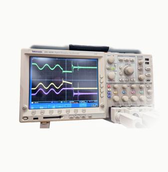
Validation and lab correlation: Use TDR scopes, VNA, and active probes to correlate simulation with measurement.
This structured flow allows electrical and layout engineers to work more predictably, minimizing surprise errors at integration.
Simulation Tools and Techniques
Promwad engineers use advanced EDA toolchains and methodologies:
- SI simulation: Mentor HyperLynx, Cadence Sigrity, Keysight ADS
- PI analysis: Ansys SIwave, Altium PDN Analyzer
- EMC pre-check: CST, EMPro
- Eye diagram analysis: Post-layout waveform extraction from memory or SERDES nets
- Test equipment: Oscilloscopes with TDR, high-bandwidth probes, CAN/Ethernet analyzers
Simulation setup typically includes:
- IBIS model selection for drivers/receivers
- Termination strategy (series, Thevenin, AC)
- Crosstalk analysis for multi-layer boards
- Simulating clock jitter and power fluctuations
The goal is to visualize and optimize margins before fabrication.
Sample Eye Diagram Improvements
Here’s a simplified example from one of our projects involving a PCIe Gen 3 interface:
| Parameter | Initial Layout | Post-SI Optimization |
| Eye height (mV) | 212 | 390 |
| Eye width (ps) | 54 | 92 |
| BER margin improvement | – | 10⁻¹² |
Result: Signal became compliant with PCIe mask; no layout respin needed.
Another common case is DDR4:
Before: Random system crashes after extended stress test
After: Skew balanced, overshoot reduced, system passed 24-hour validation
Lessons from Measurement: Aligning Simulation with Reality
In one industrial router project:
Problem: EMI failures during lab testing above 100 MHz
SI/PI insight: Return current loop was disrupted by via stitching
Solution: Simulation revealed resonance; added stitching capacitors and refined plane geometry
The final design passed EMC pre-certification in a single iteration.
In another wearable device:
Voltage dips were traced to inadequate decoupling on power rails for a wireless chip.
Adding low-ESR MLCCs and isolating fast-switching power domains eliminated interference with RF circuitry.
Tips to Reduce Design Iterations with SI/PI
- Don’t wait for the lab: simulate early and often
- Involve SI/PI engineers during stackup and schematic phase
- Correlate your test points and simulations
- Validate worst-case operating modes and corner cases
- Simulate across temperature and voltage variations
- Document simulation setup and reuse across product families
- Cross-train layout engineers to interpret eye diagrams and impedance maps
These steps allow teams to integrate simulation-driven development — not treat it as a late-stage fire drill.
Industry Trends: SI/PI Becomes Mandatory
As devices shrink and data rates rise, design teams across industries now treat SI/PI as essential:
- Automotive: ADAS, EV gateways require PCIe, Ethernet, CAN FD — all speed-sensitive
- Industrial: TSN Ethernet, industrial automation platforms require precise clocking and clean signals
- Medical: Patient safety demands immunity from transients and radiated emissions
- Telecom: 10G/40G backplanes and modules must be qualified before deployment
SI/PI isn’t just for experts anymore — it’s a core competency for product teams.
Final Thoughts: SI/PI as a Speed Advantage
In competitive hardware development cycles, delays caused by unstable signals or unpredictable power delivery can derail entire programs. Signal and power integrity are not just about high-speed interfaces — they are about building boards that work reliably, predictably, and quickly.
At Promwad, we integrate SI/PI best practices into hardware projects from day one. From layout reviews and simulation to lab correlation and EMC validation, our team helps clients:
- Reduce costly board re-spins
- Accelerate certification processes
- Ship reliable products faster
Let’s engineer stability into your next hardware design — with simulation-led development and signal confidence built-in.
Our Case Studies

