
From Concept to Live PQC Demo — Three Companies, One Board
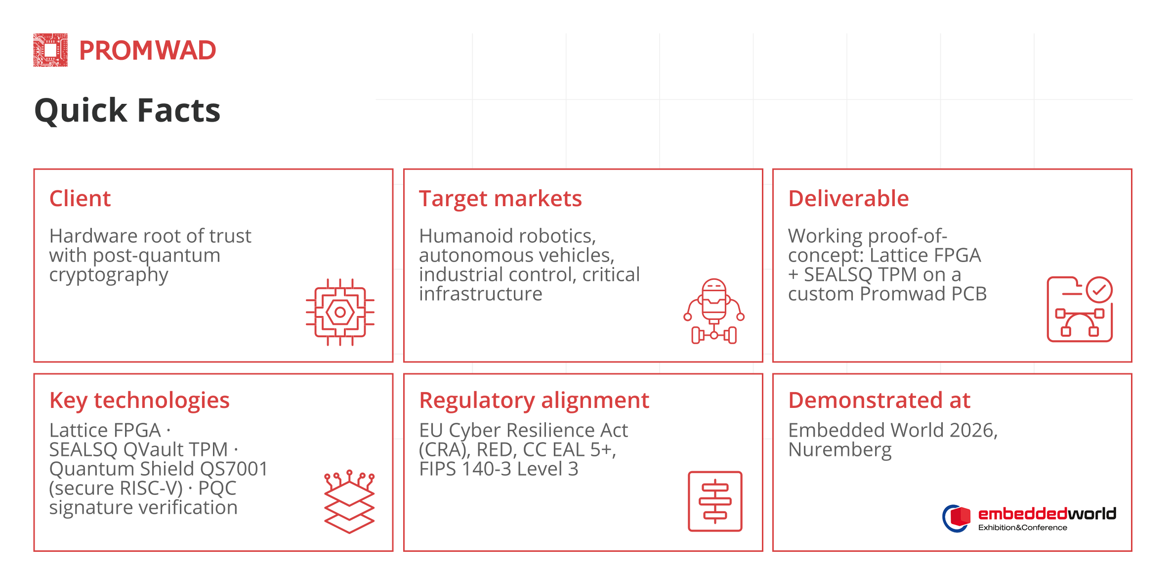
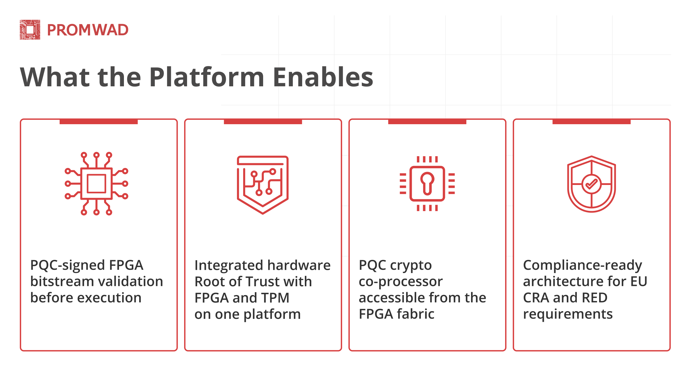
Project in a Nutshell: Promwad, Lattice Semiconductor, and SEALSQ jointly developed a hardware platform that validates FPGA bitstreams using post-quantum cryptographic signatures and demonstrated it live at Embedded World 2026. Promwad designed a custom Printed Circuit Board (PCB) integrating a Lattice Field‑Programmable Gate Array (FPGA) and a SEALSQ Trusted Platform Module (TPM) on a single board. The platform blocks unsigned or tampered firmware at the hardware level — before it ever reaches execution. The demonstrator targets edge devices with 10–20-year lifecycles in robotics, industrial automation, and critical infrastructure.
Challenge
Edge devices with 10–20-year lifecycles need cryptography that lasts just as long — but RSA and ECC won't survive the quantum era, and harvest-now, decrypt-later attacks are already making that a problem today. Meanwhile, the EU Cyber Resilience Act (CRA) and Radio Equipment Directive (RED) are raising the certification bar: static crypto architectures no longer pass.
The question: how do you anchor trust in hardware while keeping cryptographic execution updatable in the field? Lattice Semiconductor, SEALSQ, and Promwad teamed up to build a working answer.
Business Value
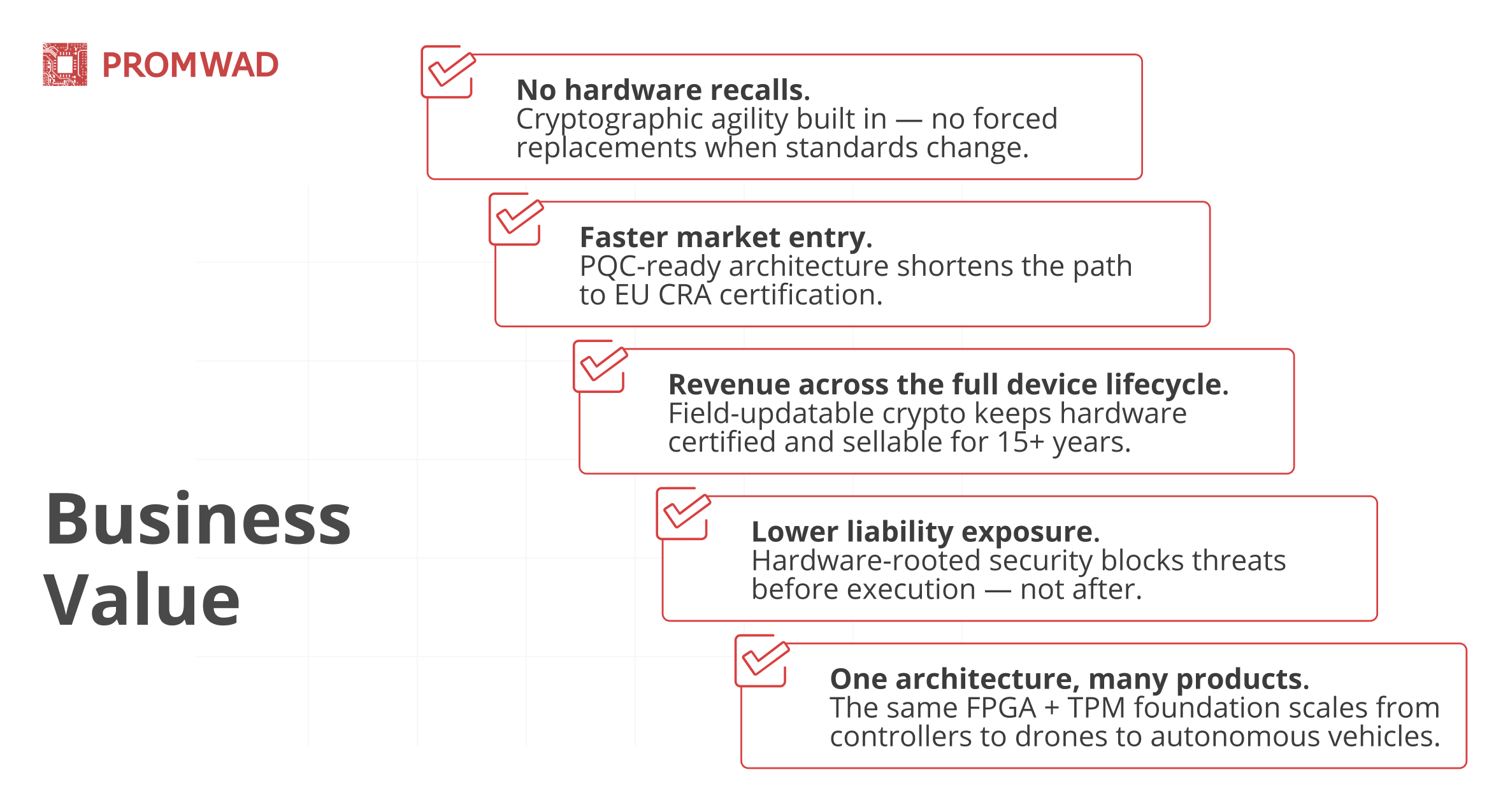
- No hardware recalls when regulations change. Devices with static cryptography face a hard choice when standards tighten: recall and replace, or lose market access. Cryptographic agility built in from the start removes that risk entirely.
- Faster entry into regulated markets. EU CRA compliance is becoming a gating requirement for connected devices in Europe. OEMs with demonstrated PQC readiness have a shorter path to certification — and a head start over competitors still retrofitting.
- Full-lifecycle revenue from the same hardware. A 15-year industrial controller that needs a hardware swap at year 7 kills margins. Field-updatable cryptography keeps the same hardware certified and sellable for its entire service life.
- Lower liability exposure. A compromised autonomous system is a product liability event, not just a technical one. Hardware-rooted security that operates below the OS shifts the narrative from "we patched it" to "it was blocked before execution."
- One security architecture across your product portfolio. The FPGA + TPM foundation is not application-specific — it scales from industrial controllers to drones to autonomous vehicles, reducing per-product security engineering costs as your lineup grows.
Solution
The three partners built a proof-of-concept platform that separates the trust anchor from the cryptographic execution layer — and proved it works on real silicon.
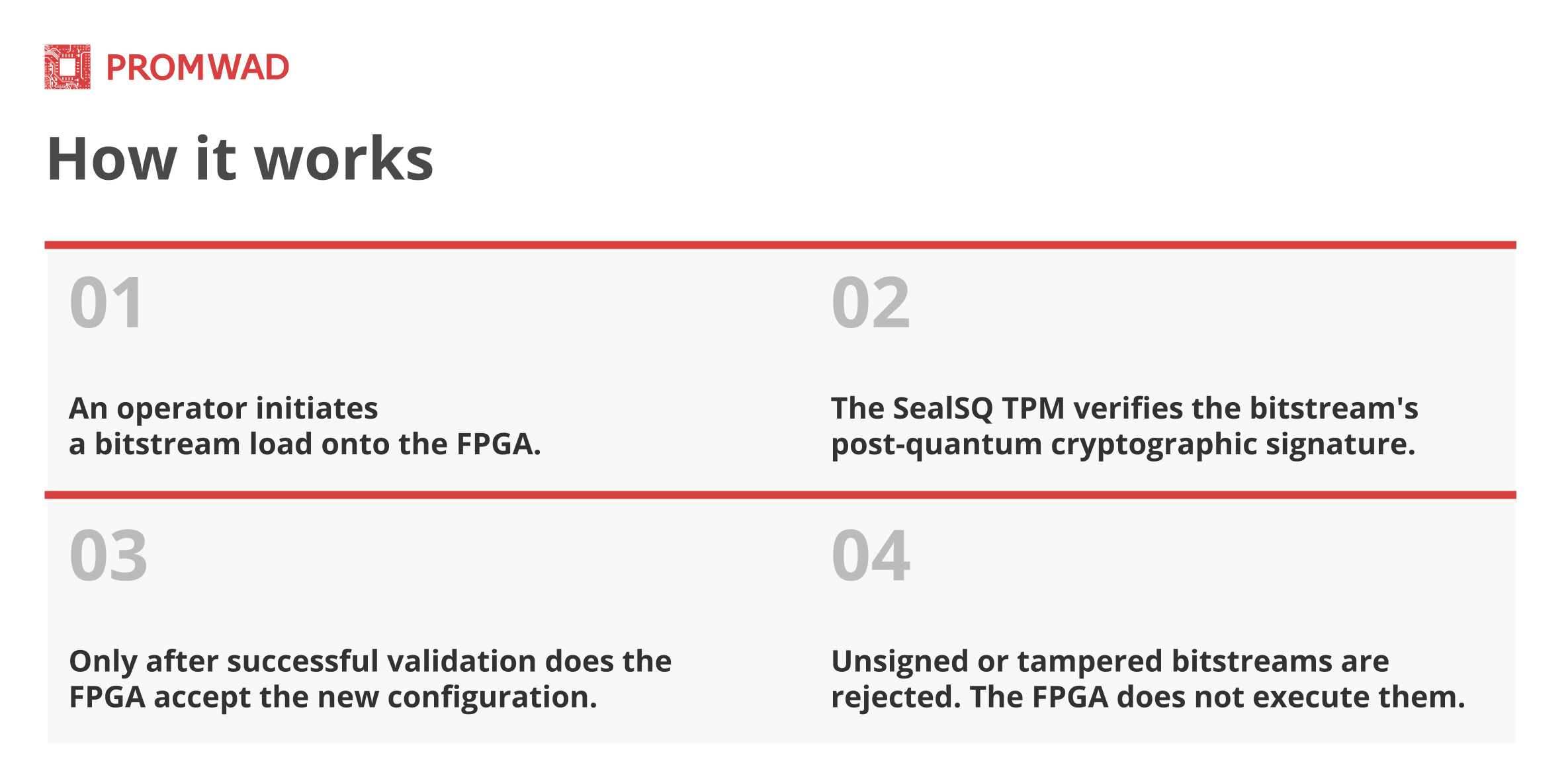
At Embedded World 2026, attendees watched this happen in real time. The board's LED display showed a hexadecimal counting sequence (0 to F) under one bitstream. When a second bitstream was loaded, the system validated its PQC signature and then switched the display to a "DONE" pattern. The demo cycled through multiple bitstreams — each validated before execution.
Architecture
The SEALSQ QVault TPM + Quantum Shield QS7001 serves as the immutable trust anchor. It stores keys, performs attestation, and runs PQC algorithms accelerated in hardware. The TPM is designed for CC EAL 5+ and FIPS 140-3 Level 3 certification. It does not change over the device's lifetime.
The Lattice FPGA provides the adaptable execution layer. It accelerates post-quantum cryptographic operations, supports algorithm agility as standards evolve, and enables field-updatable security logic — including rollback protection and anomaly filtering.
Promwad's custom PCB integrates both components on a single board. Promwad handled schematic capture, PCB layout, manufacturing release, and physical integration of all components — delivering the platform under a compressed timeline aligned to the Embedded World show date.
Why the Separation Matters
A device manufacturer can update cryptographic algorithms in deployed products — without replacing hardware and without compromising the root of trust. For a product expected to remain in service for 15–20 years, this is the difference between a single hardware generation and forced obsolescence.
Looking Ahead
This proof-of-concept is the starting point, not the end product. The architecture is designed to scale into production-grade modules for OEMs building the next generation of edge devices — from industrial controllers to autonomous platforms to humanoid robots
More of What We Do for FPGA Design
- FPGA & SoC Design Services: explore our full range of FPGA design capabilities — from RTL development and IP core integration to turnkey embedded solutions.
- FPGA Architecture Design for Home Power Inverter: check out this case study of a Lattice ECP5-based FPGA controller for a home energy management system.
- MCU vs. FPGA: Hardware Root of Trust in Embedded Cybersecurity: read our article comparing MCU and FPGA approaches to securing embedded systems.
FAQ
Do you cover the full FPGA project scope — from RTL development to PCB integration — or only the firmware side?
We cover the full stack: RTL and IP core development, high-speed PCB design with DDR4, JESD204b, and SDI interfaces, SI/PI and thermal modelling, and manufacturing release. Our tools span Vivado, Quartus Prime, and Libero — meaning we can own the entire FPGA subsystem, not just hand off a bitstream.
Are you an authorised design partner for Lattice Semiconductor, or do you work with their devices on a general basis?
We're an authorised Lattice design partner, with hands-on experience across the iCE40, MachXO3, and ECP5 families — covering use cases from small form-factor edge devices to control and security applications. That partner status means priority access to technical support and early-stage resources, which matters on tight timelines. More on our Lattice work here.
What does "end-to-end FPGA design" actually mean in practice — where does the scope start and end?
It starts at architecture: evaluating the project requirements, selecting the right platform, and defining the IP core structure. From there it covers RTL development, IP core integration, interface controller and processor core implementation, and data processing algorithm design. On the hardware side — schematic capture, high-speed PCB layout with SI/PI and thermal analysis, and full manufacturing release. The scope ends when the board works on real silicon, not when the firmware compiles.
Can you use FPGA in power electronics projects?
Yes. Promwad designs FPGA-based control and signal-processing solutions for power electronics, including PWM algorithms, feedback control loops, precise regulation, and hardware-level fault detection for real-time protection and response.
Can FPGA-based designs be updated in the field when requirements or standards change, without a hardware recall?
That's one of the core advantages of FPGA over fixed-logic solutions. The programmable fabric can be reconfigured with a new bitstream — updating algorithms, protocols, or security logic — without touching the physical hardware. For industrial devices with long service lives, this means a single hardware generation can remain compliant and functional as requirements evolve. We design with that lifecycle flexibility in mind from the architecture stage.