What a DFM Review Actually Finds — and Why It Finds It Late
One board in three. That's roughly what a contract manufacturer reports seeing when a client skips meaningful DFM review and goes straight to production. About 30% of boards fail first-pass quality control. The client blames the assembly house. The assembly house points back at the design files. Both are partly right, which is exactly why the problem keeps happening.
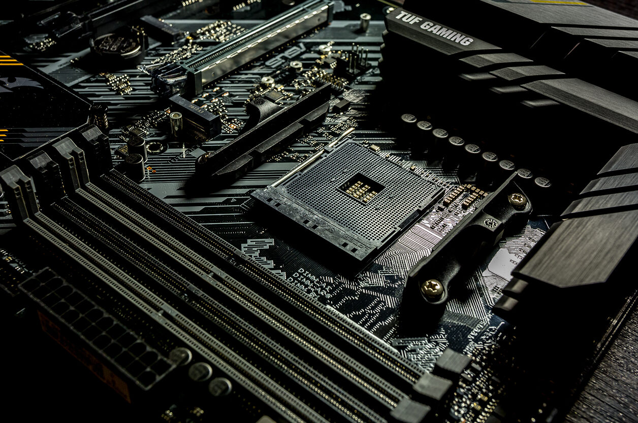
DFM review isn't about checking whether a design works electrically. The schematic can be flawless, the firmware solid, the power delivery carefully calculated — and the board can still fail at volume because the stencil aperture deposits too much paste under a QFN, because a 0402 component tombstones due to asymmetric thermal loading, or because BGA vias weren't tented and solder wicks down the barrel during reflow. None of this shows up in simulation. All of it shows up on the assembly line, usually at the worst possible moment.
What DFM actually is, precisely: it's the gap between what passes design rule check (DRC) and what survives production. DRC confirms minimum trace widths, clearances, hole sizes. DFM asks whether the board can be reliably manufactured at yield — not once, but at 500 units, at 5,000 units, by a factory running three shifts with operators who have never seen your design before.
This article covers what DFM reviews catch, organized by where in the production chain the problem would have appeared.
Fabrication Issues — Before a Single Component Is Placed
Fabrication defects kill the bare board. They're the most expensive class of DFM failure because no rework is possible: you scrap the panel and restart.
Annular ring violations are among the most common fabrication catches. The annular ring is the copper donut around a drilled hole — if it's undersized, drill registration tolerances can cause the drill to break through the ring edge entirely, destroying the via or pad. Standard fab processes require a minimum 0.1–0.15 mm annular ring; HDI processes can tighten this, but pushing to the absolute limit of a manufacturer's capability means any process variation produces scrap. DFM flags these early. DRC alone does not, because DRC only checks whether the design meets a specified rule, not whether that rule is achievable at the target manufacturer's actual process capability.
Drill-to-copper clearance is a related issue. The drill bit has a position tolerance — typically ±0.05–0.1 mm depending on the process — so the copper-to-drill edge clearance in the Gerber files must accommodate that tolerance, not just meet nominal spacing. A design where a via sits 0.08 mm from an adjacent trace looks fine on screen and passes DRC. In production, the drill drifts and shorts the trace.
Other fabrication catches that DFM reviews regularly find:
- Acid traps: traces routed at acute angles (under 90°) create corners where etchant pools, over-etching the copper and creating opens. Most ECAD tools now flag these, but imported or manually edited footprints often escape the check.
- Copper-to-board-edge clearance: copper or plane pours running too close to the board edge risk exposure and shorting after routing or V-score separation. The IPC minimum is typically 0.25–0.5 mm depending on process.
- Slivers: very thin copper features — often remnants of ground pour cutouts near pads — can detach during etching and float as conductive debris onto other boards in the same panel bath.
- Stack-up asymmetry: a multilayer board with copper distributed unevenly across layers will bow during reflow. The different thermal expansion coefficients of copper, FR4 core, and prepreg create mechanical stress when heated asymmetrically. A symmetrical stack-up — layer pair mirrored from the center outward — is the fix. This is a design decision made at stack-up selection, not fixable in Gerber post-layout.
- Aspect ratio violations: the ratio of board thickness to drill diameter has a plating reliability limit. Exceeding roughly 10:1 (board thickness to hole diameter) means the electroplating process can't reliably coat the barrel wall uniformly, resulting in weak vias that fail under thermal cycling. A 2.4 mm board with a 0.2 mm hole sits at 12:1 — marginal for standard processes.
Assembly Issues — What Kills Yield on the SMT Line
This is where most DFM findings land, and where the interaction between design decisions and production reality is most visible.
Tombstoning is a textbook case of a design-driven defect. A small passive — 0402 resistor, 0201 capacitor — lifts off one pad during reflow and stands vertical, creating an open circuit. The mechanism: solder on one pad melts and wets slightly before the other, creating an imbalanced surface tension that pulls the component upright. The design causes it through asymmetric pad geometry, mismatched trace widths entering each pad (a wide trace acts as a heat sink and delays that pad's solder melt), or proximity to a copper pour on one side only. DFM catches this by checking pad symmetry, trace width balance, and thermal relief consistency. No amount of reflow profile adjustment reliably fixes a fundamentally asymmetric pad design at volume.
QFN thermal pad voiding is less dramatic but structurally serious. The exposed pad under a QFN or power IC is meant to conduct heat from the device into the board. If the stencil aperture covers the entire pad, the paste has nowhere to outgas during reflow — flux volatiles get trapped, forming voids. Voids above 25% of the pad area (the IPC-7093 threshold for many applications) compromise thermal resistance enough to cause device overheating in the field. The fix is a windowpane or crosshatch stencil aperture pattern that reduces total paste coverage to 50–70% of the thermal pad area, leaving paths for gas to escape. DFM reviews catch this when the stencil design isn't specified or the footprint includes a single full-coverage aperture.
BGA via-in-pad is a persistent problem in high-density embedded designs. When routing space is tight, vias get placed directly in BGA pads — which is a valid technique, but only with specific process controls: the via must be filled with resin and plated over (VIPPO — Via-in-Pad Plated Over), creating a flat solderable surface. An unfilled via in a BGA pad causes solder to wick down the barrel during reflow. The ball collapses, the joint is insufficient, and the connection is intermittent — one of the hardest failure modes to diagnose because it may only manifest under thermal stress or vibration. Manual visual inspection misses over 95% of bridging and joint defects in sub-0.8 mm pitch BGAs. X-ray is required. DFM catches unfilled via-in-pad during layout review, before the Gerbers go out.
Common assembly findings in DFM reviews:
- Insufficient solder mask dams between fine-pitch pads — minimum 4 mil mask web required for standard processes; below this, bridging risk rises sharply during reflow
- Silkscreen overlapping pads — silkscreen ink on a pad prevents solder wetting; also causes stencil aperture interference where ink thickness displaces paste volume
- Components placed too close to board edges or tall neighbors — pick-and-place nozzles need clearance, and rework stations need access; 1 mm clearance around tall components is the practical minimum
- Inconsistent component orientation — polarized passives (electrolytic capacitors, tantalums, diodes) and fine-pitch ICs should be oriented consistently across the board so the reflow profile and conveyor direction apply uniformly; random orientations increase tombstoning and placement error rates
- Missing or misplaced fiducials — the pick-and-place machine uses fiducial marks on the board for registration; a board with no fiducials, or fiducials too close to the edge, will have placement accuracy degraded across the entire build
Stencil Design — The Hidden Variable
Many firmware engineers and even hardware designers treat stencil design as the assembly house's problem. It isn't. The stencil is derived from your Gerber files, and if those files don't specify aperture modifications, the house makes a 1:1 stencil — the aperture matches the copper pad exactly. That's wrong for nearly every component type.
Stencil thickness is a board-wide parameter, and it's set to the finest pitch component on the board. A 100–130 µm stainless stencil fits most mixed-technology boards. For 0.4 mm pitch BGA or 01005 passives, you may need 80–100 µm. For large power pads, 80 µm starves the pad and creates cold joints. The conflict is real. The solution is a stepped stencil — thicker in the large-pad areas, thinner in the fine-pitch areas — or a segmented paste print process. DFM review identifies this conflict at design time, when it can inform a stencil procurement decision rather than a production crisis.
Aperture modifications that DFM should specify:
- QFN/IC thermal pads: windowpane pattern, 50–70% area coverage
- Fine-pitch IC pads (< 0.5 mm): 5–10% area reduction to prevent bridging
- Small passives (0402/0201): U-shape or home-plate aperture pointing inward to reduce tombstoning force
- BGA pads: solder mask defined versus non-solder-mask defined is a separate choice affecting ball collapse behavior and must be consistent with the BGA's own pad type
One frequently missed issue: silkscreen encroachment on BGA pads. Silkscreen ink has measurable thickness — typically 15–30 µm. When it overlaps a BGA pad, it raises the stencil slightly during printing, causing excess paste to accumulate in the gap. Under reflow, that extra solder squeezes outward in the confined space between the component and the board. Microscopic bridging forms between adjacent balls — invisible to visual inspection, detectable only with X-ray. DFM catches this by flagging any silkscreen element within the solder mask opening of a BGA pad.
Testability and What Gets Missed When It Isn't Designed In
DFT (Design for Test) is technically distinct from DFM but is addressed in the same review because the cost of ignoring it lands in the same place: schedule and yield.
In-circuit test (ICT) requires test points — dedicated copper pads, typically 1 mm diameter minimum, accessible from one side of the board for a bed-of-nails fixture. On a dense embedded board, test point placement is often deferred until after routing is complete, when it's usually too late to add them without a layer respin. Boards without adequate ICT access drive up functional test time — instead of testing individual nets electrically, you test the whole board at the system level and debug from symptom to cause when something fails. On a volume production line, that's expensive per unit.
Boundary scan (JTAG, XJTAG, similar) handles the test access problem for BGAs and fine-pitch devices that can't be probed with a physical fixture. Designing JTAG chains correctly requires connecting TDI, TDO, TCK, TMS, and optionally TRST across all boundary-scan-capable devices on the board in a single chain accessible from a header or test point. This is a design decision, not a production-floor decision. DFM review checks whether boundary scan access is designed in, whether the chain is correctly ordered, and whether the programming and debug headers are accessible after the board is installed in its enclosure.
Things a DFM review checks in the testability category:
- Test points present on all critical power rails (3.3 V, 1.8 V, core voltages, reference voltages)
- Test points present on critical digital nets (SPI clock, UART TX/RX, I2C bus)
- Programming interface accessible without disassembling the enclosure
- ICT pad grid compatibility with standard fixture pin pitch (typically 100 mil or 50 mil)
- Functional test connector polarity and signal ordering matches test harness convention
- Component height clearance for bed-of-nails fixture entry from the probe side

Component and BOM Issues That DFM Reviews Catch
DFM review is also where BOM decisions meet manufacturing reality. Some component choices that look fine in ECAD create problems in production.
Non-standard package variants increase placement error risk. A footprint that diverges from the manufacturer's recommended land pattern — often because it was hand-drawn or copied from a datasheet without checking IPC-7351 — can cause misregistration, cold joints, or shorts. DFM review compares Gerber footprints against the component's actual package dimensions and IPC land pattern recommendations.
Single-source components create lead time risk that isn't a DFM issue in the traditional sense, but experienced contract manufacturers flag them because a 26-week lead time on one component blocks production of an otherwise complete board. DFM review is the right moment to ask whether an equivalent exists and whether the footprint can accommodate a second-source package.
Mixed SMT/through-hole assembly on both sides of a board adds process steps. Every additional solder process — selective soldering, wave soldering pass, hand soldering — adds cost and defect opportunity. DFM review counts the distinct assembly operations required and identifies whether component selection changes could consolidate them. Moving a through-hole connector to a press-fit variant eliminates one soldering step entirely. Not always possible, but worth asking during review rather than after the process plan is locked.
A consolidated DFM check matrix by issue category:
| Category | Typical finding | Production consequence if missed |
| Fabrication | Annular ring under minimum, acid trap, asymmetric stack-up | Scrapped panel, board warpage |
| Assembly — soldering | Tombstoning risk, QFN void, BGA via wicking | Open joints, thermal failures, intermittent connects |
| Stencil design | Missing aperture mods, silkscreen on BGA pad | Bridging, voids, paste starvation |
| Testability | Missing test points, inaccessible programming header | Increased test cost, field debug difficulty |
| BOM/component | Non-IPC footprint, single-source, mixed-process cost | Placement errors, lead time risk, assembly cost |
Quick Overview
DFM review is the process of checking whether an embedded hardware design can be reliably produced at yield — not just whether it functions electrically. It catches four categories of issue: fabrication problems (annular ring violations, drill tolerance, stack-up asymmetry, acid traps), assembly problems (tombstoning from asymmetric pads, QFN void from full-coverage stencil apertures, BGA solder wicking from unfilled via-in-pad), stencil design problems (missing aperture modifications, silkscreen overlapping BGA pads), and testability gaps (missing ICT points, inaccessible programming headers). Running DFM at placement stage costs an afternoon. Running it at Gerber release costs a respin. Skipping it can cost 30% of first-pass yield.
Key failure modes that DFM catches:
- Tombstoning of 0402/0201 passives due to asymmetric pad geometry or mismatched trace widths
- QFN/power IC thermal pad voids above 25% — thermal resistance increase causes device overtemperature in field
- BGA solder wicking through unfilled via-in-pad — intermittent connection, detectable only by X-ray
- Silkscreen encroachment on BGA pads — stencil lift causes excess paste, sub-0.8 mm pitch bridging invisible to visual inspection
- Board warpage from asymmetric copper stack-up — BGA balls lose contact during reflow
- Annular ring breakout from drilling tolerance on undersized rings — via destroyed, entire panel scrapped
- Missing solder mask dams on fine-pitch ICs — bridging between adjacent pins under standard reflow
Challenges
DFM review done by the assembly house after Gerber submission is reactive, not preventive. Houses check for what blocks their ability to build the board; they may not flag issues that reduce yield or increase field failure rates. Running independent DFM during layout — using tools such as Valor, CAM350, or Ansys Sherlock — gives the design team visibility before the file leaves the building. The cost of meaningful DFM tooling and the time required for an experienced reviewer to work through a dense embedded board are the primary barriers, particularly for small teams.
Outlook
DFM tools are moving toward inline integration in ECAD — Altium, Cadence Allegro, and Zuken CR-8000 increasingly incorporate manufacturer-specific DFM rule sets that flag issues in real time during layout rather than as a post-completion check. AI-assisted DFM analysis, applied to Gerber files and BOMs against a database of historical assembly defects, is beginning to identify non-obvious risk combinations (specific component adjacency patterns, thermal mass mismatches under particular reflow profiles) that rule-based tools miss. The direction is toward DFM that runs continuously during design rather than as a gate at the end of it.
Related Terms
DFM, design for manufacturability, DFA, design for assembly, DRC, design rule check, DFT, design for test, ICT, in-circuit test, bed of nails, boundary scan, JTAG, VIPPO, via-in-pad plated over, via-in-pad, BGA, ball grid array, QFN, tombstoning, Manhattan effect, solder bridge, solder void, reflow, reflow profile, stencil, stencil aperture, windowpane aperture, paste volume, solder paste, SPI, solder paste inspection, AOI, automated optical inspection, AXI, X-ray inspection, annular ring, drill tolerance, acid trap, copper stack-up, board warpage, bow and twist, FR4, prepreg, Gerber, CAM, ECO, IPC-2221, IPC-7351, IPC-7093, J-STD-001, fiducial, panelization, mouse-bite, V-score, surface finish, ENIG, HASL, solder mask dam, thermal relief, copper pour, hot bar, selective soldering, first-pass yield, assembly respin, EMS, contract manufacturer
Our Case Studies


FAQ
What is the difference between DRC and DFM, and why does passing DRC not mean the board is manufacturable?
DRC (design rule check) verifies that a design meets a predefined set of rules — minimum trace width, via size, clearance between copper features. These rules are set in the ECAD tool and typically reflect industry minimums or the designer's own standards. DRC flags violations. What it doesn't do is model the actual manufacturing process: how much drill position tolerance the chosen fab house has, whether the stencil aperture deposits the right paste volume for the specific component footprint, whether asymmetric pad geometry causes tombstoning during a specific reflow profile. DFM checks whether the board will yield reliably at the target manufacturer, under real process variation. A design can pass every DRC rule and still have a 30% first-pass yield failure rate in production.
Why do QFN thermal pads require windowpane stencil apertures rather than full-coverage apertures?
The QFN thermal pad is a large, flat pad with no gap for gas to escape during reflow. When flux in the solder paste heats up, it volatilizes — the vapor needs to leave the joint before the solder solidifies. A full-coverage aperture prints a continuous slab of paste with no exit paths. The vapor gets trapped, forming voids — gas bubbles in the solidified joint. Voids above roughly 25% of the pad area (per IPC-7093) increase thermal resistance enough to cause device overtemperature in applications with significant heat dissipation. A windowpane or crosshatch aperture pattern reduces total paste coverage to 50–70%, creating channels through which flux vapor can escape. The result is the same solder volume in total but distributed in a pattern that allows void-free coalescence.
What makes via-in-pad a manufacturing problem, and when is it acceptable?
An unfilled via placed directly in a component pad creates a channel that draws molten solder down the barrel during reflow — solder wicks away from the joint surface, leaving an insufficient ball collapse or an open. For BGA pads this produces intermittent connections that survive basic electrical test but fail under thermal stress or vibration. Via-in-pad is acceptable when the via is filled with non-conductive or conductive epoxy and then plated over, creating a flat, continuous pad surface. This process is called VIPPO (Via-in-Pad Plated Over) and adds cost — typically $0.10–$0.50 per via depending on volume. DFM review flags unfilled or capped-but-not-plated via-in-pad on any fine-pitch component, particularly BGAs and QFNs.
At what stage of the design process should DFM review happen?
The answer most engineers give is "before Gerber release." The answer that avoids respins is earlier: targeted DFM checks should run at multiple stages — after component selection (to flag package choices that create assembly conflicts), after initial placement (to check component spacing, orientation, and thermal balance), and comprehensively before routing is locked (so that testability findings, via-in-pad conflicts, and stack-up decisions can still be changed without a full layout redo). DFM at Gerber release catches problems, but at that stage fixing them costs an ECO, a board respin, and typically 2–4 weeks. DFM at placement stage catches the same problems when they cost an afternoon of layout work.