Power Integrity in High-Density Embedded Boards: PDN Design When AI Workloads Hit the Same Rail

A neural processing unit firing up an inference pass draws current differently from anything a traditional embedded board was sized to handle. The NPU's MAC array activates in a coordinated burst — thousands of multiply-accumulate units switching simultaneously — and the resulting current transient is steep, localized, and repeating at the cadence of the inference pipeline. When this happens on a power rail shared with the application CPU, memory interfaces, and peripheral logic, the PDN that seemed adequate during static power budgeting becomes the first place the system fails under real operating conditions.
This is not a data center problem that has migrated to the edge. It is a new PDN design constraint that appeared with the integration of dedicated AI accelerators into embedded SoCs. STMicroelectronics' STM32N6 series, which embeds the Neural-ART Accelerator NPU into a microcontroller-class device, delivers 600 times the machine learning throughput of a high-end STM32 without an NPU. Qualcomm's QCS8550, Rockchip RK3588, and NXP i.MX 95 all integrate NPU or ML-acceleration blocks alongside general-purpose CPU cores on a single die. Every one of these platforms creates a new set of power delivery requirements that need to be addressed before the first prototype is assembled.
How AI Inference Loads Differ from Conventional Embedded Workloads
Traditional embedded workloads — sensor polling, communication stack processing, motor control loops — produce gradual, predictable current draw with moderate peak-to-average ratios. The VRM has time to respond, decoupling capacitors provide bridging charge during brief transients, and the power rail stays within tolerance without aggressive PDN engineering.
AI inference introduces a fundamentally different load profile. The NPU's compute array is idle between inference calls and then activates all its processing elements simultaneously when a frame or data batch is ready. The transition from idle to full compute load happens in nanoseconds to microseconds — faster than any VRM feedback loop can respond. The current step is proportional to the number of active MAC units and their switching frequency. On a mid-range edge AI SoC, this transition can represent a current step of several amperes on the NPU core rail within a single microsecond.
The problem compounds when the NPU shares a rail with the application CPU. A common scenario in cost-sensitive embedded AI board designs places the CPU cluster and NPU on a shared power domain to reduce VRM count and PCB complexity. When an inference batch triggers the NPU at the same moment the CPU is executing a memory-intensive task, the combined transient current demand can exceed the sum of each component's individual peak by a meaningful margin due to the overlapping activation patterns. This is the condition under which underdamped power rails ring, voltage droops exceed the SoC's specification, and the system produces intermittent compute errors that are extremely difficult to reproduce in isolation.
The key parameters that define an embedded AI board's power delivery challenge are:
- Peak transient current magnitude: the amperage step when the NPU activates from idle
- Transient rise time: how quickly the current step occurs, measured in nanoseconds
- Repetition frequency: how often inference batches arrive, driven by the application pipeline
- Rail sharing topology: which other logic blocks share the affected supply domain
- SoC voltage tolerance: the allowed droop on the core supply, typically ±3 to 5 percent on modern process nodes
Target Impedance — The Fundamental Design Metric
The PDN's job is to deliver current to the SoC while holding the supply voltage within the specified tolerance window. The target impedance, expressed in milliohms, is the maximum impedance the PDN can present to the load across the full frequency range of interest while satisfying that voltage tolerance. For an embedded AI SoC operating at a 1.0V core rail with a ±5% tolerance and a peak transient current of 5A, the target impedance is 10mΩ. If the PDN impedance exceeds 10mΩ at any frequency where the load draws current, the voltage droop exceeds specification.
The frequency range of interest spans from DC up to several hundred megahertz, covering the full spectrum of transient frequencies generated by the load. Each element of the PDN contributes to the impedance profile over a different frequency range:
| PDN element | Dominant frequency range | Primary contribution |
| VRM / switching regulator | DC to ~100 kHz | Low-frequency impedance, output capacitance |
| Bulk capacitors (47–470 µF) | 1 kHz – 1 MHz | Mid-frequency bulk charge reservoir |
| MLCC mid-range (1–10 µF) | 100 kHz – 50 MHz | Bridging between bulk and high-frequency |
| MLCC high-frequency (0.1 µF) | 10 MHz – 200 MHz | High-frequency decoupling near SoC |
| PCB plane capacitance | 100 MHz – 1 GHz | Very high frequency, layout dependent |
| Package and on-die capacitance | 500 MHz and above | Fastest transients, set by silicon |
The impedance profile resulting from these elements is not flat. Anti-resonances appear at frequencies where the inductance of one capacitor tier resonates with the capacitance of an adjacent tier, creating impedance peaks that can be several times higher than the DC impedance. A classic embedded PDN anti-resonance, the Bandini Mountain, appears where the mounting inductance of the board-level MLCCs resonates with the package capacitance of the SoC. If this peak lands at a frequency where the NPU generates significant transient energy, the voltage droop during inference can be several times larger than simple DC IR-drop calculations would predict.
Managing this requires knowing not only the SoC's static current draw but the frequency content of its transient current. Some SoC vendors provide this information in power integrity application notes. For devices where it is not documented, the practical approach is to characterize the load current waveform on a reference board using a current probe or shunt measurement before committing the production PDN design.
VRM Selection and Placement for AI SoC Boards
The voltage regulator module is the slowest element in the PDN. A typical synchronous buck converter with a 500 kHz switching frequency has a control loop bandwidth of roughly 50–100 kHz. Below this frequency, the VRM actively regulates and maintains the output voltage. Above this frequency, the VRM is effectively an inductor in series with its output capacitors from the load's perspective — it cannot respond fast enough to supply the transient current, and the decoupling capacitors on the board must provide it instead.
This means the VRM's primary role for AI workloads is not to supply the inference burst — it cannot do that fast enough — but to replenish the charge drawn from the decoupling network after the burst ends, and to set the correct average voltage for the rail. The VRM specification for a high-performance edge AI board needs to address:
- Output current rating with sufficient margin above the sustained load: for an SoC pulling 15A peak during inference, a 20A VRM provides minimal headroom; a 25–30A device gives appropriate margin for thermal and aging derating
- Transient response specification: the VRM datasheet's load step response characterizes how quickly the output recovers after a large current step, which determines the bulk capacitance required to keep the droop within tolerance during that recovery period
- Switching frequency: higher switching frequencies allow smaller output inductors, which improves transient response bandwidth at the cost of switching losses; multi-phase operation distributes heat and effectively multiplies the switching frequency seen by the output filter
Physical placement of the VRM on the board has a direct impact on PDN performance. Every centimeter of PCB trace between the VRM output and the SoC power pins adds loop inductance to the power delivery path. At the current levels and transient rates of an AI SoC, loop inductance produces voltage ringing that appears as noise on the supply rail. The VRM should be placed as close to the SoC power pins as the mechanical and thermal constraints allow, with a dedicated power plane pour between the two rather than a traced connection.
On SoMs and carrier board designs — a common architecture for edge AI products where the compute module is a separate PCB mated to an application board — the VRM placement problem becomes more complex. If the VRM is on the carrier board and the SoC is on the module, the inter-board connector inductance adds directly to the PDN loop inductance for the highest-frequency transients. Designs targeting AI inference workloads benefit from placing the core VRM on the SoM itself, as close as possible to the SoC, and using the carrier board connector only for the input bus voltage rather than the regulated core rail.
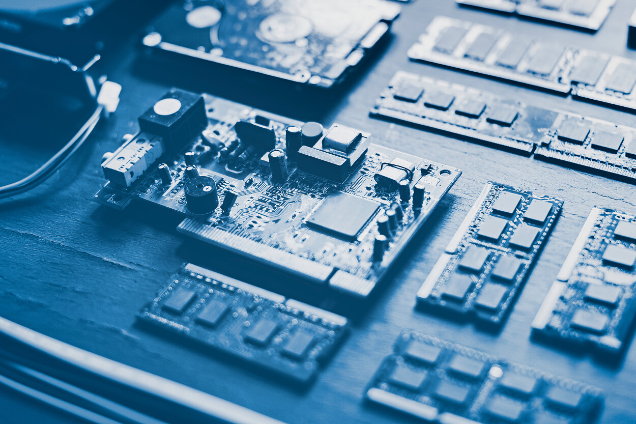
Decoupling Strategy for NPU Transient Currents
The decoupling network for an AI SoC board needs to be designed explicitly for the NPU's transient profile rather than inherited from a previous-generation board that did not include an AI accelerator. The common mistake is to use the same decoupling count and placement as a similar-class SoC without an NPU and add a margin factor. This approach leaves impedance peaks unaddressed because it does not account for the different frequency content of AI inference transients.
A structured approach to decoupling for AI workloads involves three tiers:
First tier: bulk capacitance adjacent to the VRM output. Electrolytic or polymer capacitors in the 47 to 470 µF range supply charge during the VRM's recovery time after a large load step. The quantity is set by the required voltage hold-up during the VRM response time — a VRM with a 10 µs recovery time holding a 1V rail within 50 mV while supplying a 5A step needs at least 1000 µF of bulk capacitance. Polymer capacitors are preferred over electrolytics in high-temperature embedded applications because their equivalent series resistance (ESR) is more stable over temperature.
Second tier: mid-range MLCC capacitors between 1 and 10 µF distributed across the power plane. These bridge the frequency gap between the bulk capacitors and the high-frequency devices closest to the SoC. X5R and X7R dielectric MLCCs in 0402 and 0603 packages provide adequate capacitance density. The key constraint is that capacitance of MLCCs with X7R and X5R dielectrics decreases with applied DC bias — a 10 µF capacitor rated at 10V may deliver only 4–5 µF at its actual operating voltage. This derating must be accounted for in the impedance calculation.
Third tier: high-frequency 100 nF MLCCs with minimal equivalent series inductance (ESL), placed within 1–2 mm of the SoC power pins. These handle the fastest transients, above 10 MHz, that the mid-range capacitors cannot reach due to their higher mounting inductance. For BGA-packaged SoCs, placing decoupling capacitors in the via field beneath the package — between the BGA balls and the PCB surface — minimizes the inductance of the current path and directly addresses the highest-frequency droop at the die supply pins.
The total capacitor count should not be optimized purely by cost reduction without simulating the resulting impedance profile. PDN simulation tools including Ansys SIwave, Cadence Sigrity PowerDC, and Siemens HyperLynx can model the full impedance curve of the proposed layout before board fabrication and identify anti-resonance peaks that can be suppressed by adding targeted damping capacitors at specific locations. For AI SoC designs where the inference current profile has been characterized, injecting this profile into the simulation produces a time-domain voltage waveform that can be compared directly against the SoC's supply tolerance specification.
Layer Stack-Up and Plane Architecture
The PCB layer stack-up determines the intrinsic capacitance and inductance of the power distribution planes, which affect impedance across the mid- and high-frequency range where decoupling capacitors provide most of the PDN's performance.
A high-density embedded AI board targeting low PDN impedance above 10 MHz benefits from the following stack-up principles:
- Power and ground planes should be adjacent layers with minimal dielectric thickness between them. A 4-mil dielectric between a 1V core power plane and the adjacent ground reference provides approximately 0.5–1 nF per square inch of plane capacitance, which contributes usefully to the high-frequency PDN without requiring additional capacitor components.
- The SoC power domain planes should be as close to the top layer (component side) as the signal routing constraints allow, minimizing the via stub length and associated via inductance between the surface components and the planes.
- For a 10-layer board hosting an AI SoC with multiple power domains, a representative high-performance stack assigns the outermost signal layers to high-speed interfaces such as LPDDR and PCIe, places the SoC core power and ground planes as layers 2 and 3, and uses inner layers for secondary power domains and lower-speed routing. This minimizes the inductance of the critical core power delivery path.
Split power planes — where multiple power nets share a single physical layer with gaps separating the domains — introduce impedance discontinuities at the gap boundaries and create return path interruptions for signals crossing between domains. For high-density AI boards where this is unavoidable due to the number of power domains, the gaps should be oriented so that no high-speed signal traces cross them. A gap in a power plane under a DDR or PCIe routing channel adds inductance to the signal return path and produces EMC and signal integrity problems that compound the power integrity challenge.
Shared Rail Partitioning and Domain Isolation
As AI SoC integration increases, the temptation to reduce VRM count by sharing rails across multiple functional blocks becomes a production cost pressure that conflicts directly with power integrity requirements. The engineering framework for evaluating shared rail proposals follows a consistent logic: blocks that have correlated activity — blocks that activate simultaneously in the application workload — generate correlated transient currents that add constructively on the shared rail and amplify the droop beyond what either block would produce independently.
For an embedded vision system where the NPU fires on every camera frame and the image signal processor (ISP) processes the same frame simultaneously, placing both on the same core rail produces a compounded transient that matches the worst-case scenario the PDN must survive. The decoupling requirement for this combined transient is larger than the sum of individual requirements because the simultaneous activation reduces the available charge from the decoupling network more rapidly.
Separate VRM phases for the NPU core and the CPU cluster, even if both regulators are sourced from the same input bus, allows independent PDN sizing for each domain and eliminates the cross-domain transient coupling. The cost of the additional VRM phase is typically recovered in reduced decoupling capacitor count and eliminated board respins caused by power integrity failures discovered late in validation. Engineering teams working across hardware design and embedded systems integration, including those that develop AI-enabled embedded products from concept to mass production, find that the decision to share or isolate rails needs to be made in the platform architecture phase, before schematic capture, based on actual application workload analysis rather than optimistic average-power estimates.
Quick Overview
Power integrity design for embedded AI boards must address the current transient profile of integrated NPUs and AI accelerators, which differs fundamentally from conventional embedded workloads. NPU activation produces fast, high-magnitude current steps that the VRM cannot supply directly — the decoupling network must bridge the transient while the VRM recovers. Target impedance across the full frequency spectrum from DC to hundreds of megahertz defines the design requirement, and anti-resonance peaks in the PDN impedance profile are the primary failure mechanism in underdamped designs.
Key Applications
Edge AI vision systems using SoCs with integrated NPUs such as Rockchip RK3588, NXP i.MX 95, or STM32N6, industrial AI boards running inference pipelines on shared CPU-NPU power domains, SoM-based embedded AI platforms where VRM placement is constrained by the module-carrier board boundary, high-density embedded computing modules targeting AI workloads in automotive, robotics, and industrial inspection.
Benefits
Explicit PDN simulation using the NPU transient current profile as the excitation source identifies impedance peaks and decoupling gaps before board fabrication, eliminating power-integrity-related board respins. Separating NPU and CPU core supply domains with independent VRM phases removes cross-domain transient coupling and reduces the peak decoupling requirement for each domain. Adjacent power and ground plane pairs with minimal dielectric thickness provide plane capacitance that supplements the discrete decoupling network at frequencies above 100 MHz without requiring additional components.
Challenges
DC bias derating of X5R and X7R MLCC capacitors at operating voltage significantly reduces effective capacitance relative to nominal ratings, and must be explicitly accounted for in impedance calculations. VRM feedback loop bandwidth limits its ability to supply fast AI inference transients, placing the full burden of transient response on the decoupling network. SoM-based designs introduce inter-board connector inductance into the highest-frequency PDN path if the VRM is on the carrier board. NPU transient current profiles are not consistently documented by SoC vendors, requiring board-level current measurement characterization on reference hardware.
Outlook
Integration of NPUs into microcontroller-class and mid-range embedded SoCs continues to increase, bringing AI inference transient power requirements into product categories — industrial sensors, embedded vision modules, edge gateways — where PDN engineering has historically been straightforward. Point-of-load VRM integration into SoC packages, active on-die voltage regulation, and embedded passive technologies that reduce decoupling capacitor mounting inductance are all advancing to address the power delivery challenge at the silicon level. For boards produced in the near term, the PDN engineering burden remains with the hardware team and requires explicit simulation and characterization rather than rule-of-thumb decoupling density from prior non-AI designs.
Related Terms
PDN, power delivery network, target impedance, VRM, MLCC, ESR, ESL, DC bias derating, Bandini Mountain, IR drop, decoupling capacitor, NPU, neural processing unit, edge AI, AI inference, switching regulator, buck converter, power plane, layer stack-up, SoM, BGA decoupling, transient current, anti-resonance, power integrity simulation, Ansys SIwave, Cadence Sigrity, HyperLynx, LPDDR power domain
Our Case Studies


FAQ
What is target impedance in PDN design and why does it matter for AI inference boards?
Why do MLCC decoupling capacitors lose capacitance on AI SoC boards?
How does VRM placement on an embedded AI board affect power integrity?
What causes the Bandini Mountain resonance in embedded PDN designs?
How does IPMX change the test matrix compared to ST 2110?
What should I store as evidence from automated runs?