Choosing the Optimal Edge Device Architecture in Resource-Constrained Environments: MCU, SoC, FPGA, and Hybrid Platforms in 2026
The architecture selection decision for an embedded edge device is one of the earliest and most consequential design choices an engineering team makes. It determines what compute the device can perform, what firmware complexity it can support, what power budget it requires, and what its unit cost and BOM structure will be. Made correctly at the beginning of the project, it sets the design on a path where firmware, hardware, and certification efforts align. Made incorrectly, it produces either an underpowered system that cannot execute the required workload, or an over-specified system that consumes 10x the required power and costs 5x what the product's margin structure can absorb.
In 2026, the architecture selection landscape has shifted significantly from even two years ago. MCUs now incorporate dedicated neural processing units — TI announced the MSPM0G5187 and AM13Ex MCU families with integrated TinyEngine NPUs at Embedded World 2026, making edge AI a standard capability in new MCU designs rather than a SoC-exclusive feature. SoCs have converged toward integrated NPUs, multi-protocol wireless, and hardware security modules in a single chip, reducing BOM complexity at every tier. And FPGA vendors are advancing AI toolchains specifically to close the RTL expertise gap that historically limited FPGA adoption. The result is an architecture landscape where the decision boundaries have shifted and the conventional rules of thumb from five years ago require revision.
This article covers the specific technical decision criteria for each architecture class, the 2026 silicon options at each tier, the hybrid combinations that serve the most demanding applications, and the decision framework that matches architecture to application requirements.
The Architecture Decision Is a Systems Engineering Problem
Architecture selection errors produce a specific class of problem: one that cannot be fixed by firmware optimization or component substitution. An MCU selected for an application that requires Linux cannot run Linux — it lacks the memory management unit and minimum RAM required. An SoC selected for a real-time motion control application may miss hard deadlines due to OS scheduling jitter. An FPGA selected to save cost at high volume adds $8–12 per unit in BOM and 3 months to development time for a capability that a $2 SoC could provide.
The cost of an architecture revision — replacing the primary silicon — is the most expensive engineering change possible after PCB layout is committed. It requires a new schematic, a new layout, new firmware bring-up, and often new regulatory testing. The NRE for an architecture change at the prototype stage typically ranges from $30,000–$100,000 plus 6–12 weeks of schedule.
Architecture selection must be treated as a systems engineering decision driven by quantified requirements, not by team familiarity or vendor relationships.
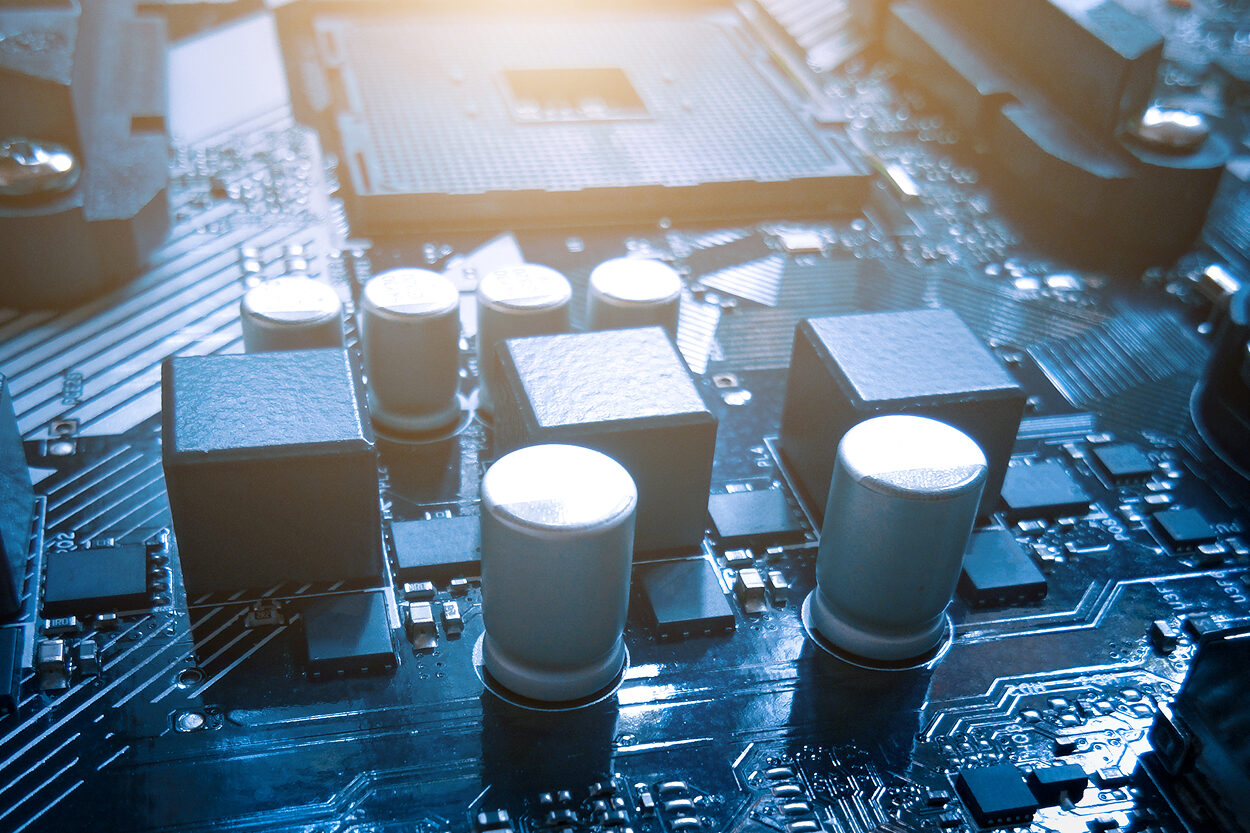
MCUs — Ultra-Low Power and TinyML in 2026
MCUs remain the correct choice for a large class of embedded applications: ultra-low power operation on battery or energy harvesting, simple sensor acquisition and conditioning, control loops without AI processing requirements, and cost-sensitive IoT node designs where BOM budget is $1–5 per unit.
The significant change in 2026 is that AI capability has moved into MCU silicon. TI's MSPM0G5187 and AM13Ex MCUs integrate the TinyEngine NPU, enabling efficient deep learning inference at MCU power levels — enabling keyword detection, anomaly detection from sensor data, gesture recognition, and simple image classification without requiring an external AI accelerator or an upgrade to SoC-class silicon. TI's CCStudio Edge AI Studio provides more than 60 models and application examples for deployment on these MCUs. ARM's Cortex-A320 with Ethos-U85 NPU now supports efficient transformer operator execution, with ARM positioning the platform for on-device models approaching one billion parameters on IoT-scale devices.
This changes the architecture decision for a specific class of applications: sensor-based anomaly detection, keyword spotting, predictive maintenance on constrained hardware, and simple vision classification tasks that previously required upgrading to an application processor. These tasks can now remain in MCU-class silicon, preserving the sub-mW power profile and sub-$5 unit cost that MCU designs deliver.
MCU limitations that do not change with NPU integration: no MMU means no Linux; constrained RAM (typically 256KB–2MB) limits model size; single-threaded RTOS or bare-metal execution limits multi-task complexity. These remain hard constraints. NPU-equipped MCUs expand the AI capabilities of MCU designs, but they do not change the fundamental architectural boundary between MCU and SoC.
Current MCU options for AI-capable embedded designs
| MCU family | NPU/AI capability | Key specs | Target applications |
| TI MSPM0G5187 | TinyEngine NPU | ARM Cortex-M0+, 2MB flash | Industrial sensing, TinyML |
| TI AM13Ex | TinyEngine NPU | Cortex-M33, 512KB RAM | Factory automation, anomaly detection |
| STM32N6 | Neural-ART NPU | Cortex-M55, 4.2MB RAM | Vision, sensor fusion |
| Nordic nRF54 series | DSP-accelerated | Cortex-M33, BLE/BT, 1MB RAM | IoT, wearables, connected sensors |
| STM32U5 | eXtended DSP (no NPU) | Cortex-M33, 786KB RAM | Ultra-low power IoT |
| Ambiq Apollo4 | AI accelerator | Sub-mW active | Wearables, always-on sensing |
SoCs — Application Processors with Integrated AI
SoC-class application processors are appropriate when the application requires Linux or a full OS, high compute throughput for multimedia or complex AI, rich connectivity (cellular, Wi-Fi 6, gigabit Ethernet), or display interfaces. SoCs integrate CPU cores, GPU, NPU, connectivity blocks, and security subsystems in single silicon — the integration reduces BOM complexity relative to MCU + discrete peripheral designs at the cost of higher power consumption and greater firmware development complexity.
The 2026 SoC landscape has converged on integrated NPUs as a standard feature rather than a premium option. The NXP i.MX 8M Plus integrates an 2.3 TOPS NPU for vision and voice workloads alongside quad Cortex-A53 cores. The Rockchip RK3588 delivers 6 TOPS NPU performance for edge AI alongside 8 CPU cores. Qualcomm's RB5 platform targets robotics and industrial applications requiring 5G connectivity alongside AI inference. ARM's Cortex-A320-based platform with Ethos-U85 NPU represents the emerging generation of tightly integrated CPU-NPU designs targeting milliwatt-level AI inference.
The SoC selection decision involves a different set of tradeoffs than MCU selection. Thermal management is significant — SoCs running sustained workloads at 4–8W require thermal design that MCU products (typically <200mW active) do not. Boot time from power-on to running Linux and application code takes 3–10 seconds without optimization, which is unacceptable for applications requiring sub-second startup. Power consumption in standby — Linux suspend to RAM — is typically 10–50x higher than MCU deep sleep.
FPGAs — Deterministic Pipelines and Custom Logic
FPGAs provide capabilities that neither MCUs nor SoCs can match: true hardware parallelism, sub-microsecond latency determinism, and the ability to implement custom logic and interfaces that do not exist in standard silicon. These properties are relevant to a specific but important class of edge applications.
Real-time signal processing with deterministic latency requirements — industrial control loops closing at 10kHz or faster, high-speed data acquisition, motor control with sub-10µs interrupt response — cannot be met by software execution on either MCU or SoC. Software execution is subject to interrupt latency, pipeline stalls, and OS scheduling delays that create timing jitter. FPGA-implemented control logic executes in deterministic hardware clock cycles with no jitter.
Custom sensor interfaces and proprietary protocols are straightforward to implement in FPGA fabric but may require significant software workarounds on standard silicon. High-speed parallel sensor buses, custom synchronization protocols, or protocol bridging between incompatible standards (SDI to ST 2110 in broadcast, for example) are natural FPGA applications.
AI acceleration on FPGA has matured significantly in 2026. AMD's Xilinx Kria K26 (AMD/Xilinx Zynq UltraScale+ MPSoC with FPGA fabric) provides pre-built vision AI applications including object detection, classification, and tracking, with AI model integration through Vitis AI. Altera (now independent from Intel, with Silver Lake holding 51% ownership) is moving beyond data center applications toward edge AI, with the Agilex series offering claimed 2x clock rate advantages over competitors through tensor block architecture. FPGA AI toolchains are closing the gap between ML engineering (TensorFlow/PyTorch) and hardware engineering (RTL), reducing the specialist expertise barrier.
The FPGA cost tradeoff remains significant. Mid-range FPGAs suitable for production edge devices cost $8–30 in BOM, compared to $2–8 for equivalent SoC-class silicon. FPGA development tooling (AMD Vivado, Intel/Altera Quartus) requires specialized expertise beyond standard embedded software skills. For applications that genuinely require FPGA capabilities, these costs are justified. For applications where an SoC with software would meet requirements, they are not.
Hybrid Architectures
The most demanding embedded edge applications combine silicon from multiple architecture classes, assigning each subsystem to the architecture best matched to its requirements. This is not a compromise or a fallback — it is the correct architecture for products where different subsystems have incompatible requirements.
SoC + MCU is the most common hybrid pattern. The SoC handles the Linux-based application stack — networking, cloud communication, user interface, complex data processing — while the MCU handles hard real-time control loops, safety-critical functions that must remain deterministic regardless of SoC load, and ultra-low power sensor acquisition during system sleep states. A smart industrial controller might use an NXP i.MX 8M Plus for its machine-learning-based condition monitoring UI and data aggregation while an STM32 handles the safety-rated motor control loop that must meet 10µs hard deadlines.
SoC + FPGA is appropriate when the application requires both high-level software and deterministic hardware pipelines. AMD/Xilinx Zynq devices integrate both on a single chip — ARM application processors plus programmable logic in the same package — providing a clean interface between the software and hardware worlds without discrete chip-to-chip communication. External SoC + FPGA configurations on separate chips are used when the SoC provides sufficient compute for the software requirements but requires FPGA-accelerated I/O or signal processing support.
MCU + FPGA appears in applications requiring extremely low system power with custom I/O requirements — industrial sensor nodes that must implement unusual sensor interfaces while maintaining battery operation.
Architecture Decision Framework
The architecture selection follows from quantified answers to a specific set of questions. These questions must be answered before silicon is selected, not after:
| Design requirement | Architecture implication |
| Battery life target: years without replacement | MCU primary; avoid SoC wake states |
| Power budget: >1W sustained | SoC or FPGA; MCU insufficient |
| Linux required | SoC required; MCU cannot run Linux |
| AI inference: keyword/anomaly on sensor data | MCU with NPU (TinyML) |
| AI inference: vision at 30fps | SoC with NPU, or dedicated AI accelerator |
| Hard real-time deadline: <1ms | MCU or FPGA; SoC jitter unacceptable |
| Hard real-time deadline: <10µs | FPGA required |
| Custom sensor interface / proprietary protocol | FPGA or MCU GPIO bit-banging |
| Multimedia: video decode, display output | SoC required |
| OTA firmware updates | SoC (Linux) or MCU with dual-bank flash |
| EU CRA compliance (security architecture) | All tiers require hardware security; SoC/MCU with TrustZone preferred |
| BOM target: <$5 per unit | MCU; SoC rarely achieves <$5 in mass market |
| Production volume: >100,000 units | Evaluate custom SoC integration or ASIC |
The question "does the application require Linux?" is the single most decisive. Linux requires a memory management unit (MMU), a minimum of 64–128MB RAM, and boot time measured in seconds. MCUs do not have MMUs and cannot run Linux. Any application requiring a web server, complex networking stack, package manager, or user-facing software framework requires SoC-class silicon.
The question "does any subsystem have a hard real-time deadline under 1ms?" is the second most decisive. SoCs running Linux cannot guarantee sub-millisecond interrupt response times under load due to OS scheduling behavior. Hard real-time requirements under 1ms push toward MCU or hybrid SoC+MCU. Requirements under 10µs push toward FPGA.
Quick Overview
Key Applications: battery-powered IoT nodes requiring TinyML inference (MCU + NPU), smart industrial gateways with AI analytics and connectivity (SoC), real-time protocol bridges and custom-interface devices (FPGA), complex products with both hard real-time and Linux requirements (SoC + MCU hybrid), AI-accelerated vision pipelines with custom I/O (SoC + FPGA / Zynq)
Benefits: AI-capable MCUs enable TinyML at sub-mW power without SoC upgrade; SoC integration of NPU + connectivity + security in single silicon reduces BOM vs. discrete approaches; FPGA delivers deterministic sub-µs latency where SoC OS jitter is unacceptable; hybrid architectures assign each subsystem to best-matched silicon without compromise
Challenges: architecture revision after PCB layout commits costs $30,000–$100,000 and 6–12 weeks; FPGA development requires RTL expertise that most firmware teams lack; SoC boot time (3–10 seconds) unacceptable for applications requiring fast startup; hybrid architectures add firmware complexity at the SoC-MCU interface; EU CRA hardware security requirements must be designed in from the architecture stage
Outlook: TinyML moving from specialty capability to standard MCU feature (TI TinyEngine NPU, STM32N6, Ethos-U85); SoC-MCU-NPU integration continuing to increase with heterogeneous SoCs running RTOS + Linux + AI inference simultaneously; RISC-V gaining traction in custom SoC and FPGA soft-processor designs; FPGA AI toolchains closing the RTL/ML expertise gap; by 2028, embedded devices expected to ship with built-in intelligence, connectivity, and lifecycle management by default
Related Terms: MCU, SoC, FPGA, hybrid architecture, TinyML, TinyEngine NPU, Neural-ART, Ethos-U55, Ethos-U85, ARM Cortex-M55, NXP i.MX 8M Plus, Xilinx Kria K26, Zynq UltraScale+, Altera Agilex, RTOS, bare-metal, Linux embedded, hardware abstraction layer, edge AI, TensorFlow Lite Micro, EdgeImpulse, secure boot, TrustZone, EU Cyber Resilience Act, OTA firmware, BOM cost, real-time control
Our Case Studies


FAQ
When should I use a hybrid SoC + MCU architecture instead of just an SoC?
Can modern MCUs run TinyML inference, and what are the practical constraints?
When does FPGA justify its cost and complexity over SoC?
What architecture is best for EU Cyber Resilience Act compliance in connected embedded products?