Rapid Prototyping and Manufacturing of Complex Electronics: Workflows, Tools, and the Path to Production in 2026
The gap between a working prototype and a manufacturable product has always been the most expensive part of hardware development. Most schedule overruns do not occur during design — they occur at the boundary between prototype and production, where design decisions that were acceptable for ten units become manufacturing problems at ten thousand.
In 2026, the tools available to compress this gap have improved substantially. Quick-turn PCB assembly has moved from 5–7 business day cycles to 48–72 hours for standard builds, with 24-hour bare-board fabrication available when files are DFM-ready. AI-driven DFM checks collapse the traditional file review bottleneck. Digital twin platforms enable software validation and system integration before physical hardware exists — Synopsys launched an electronics digital twin platform in March 2026 that enables up to 90% of software validation prior to hardware availability. The development paradigm has shifted from sequential phase gates toward concurrent streams that overlap hardware, firmware, mechanical, and test development.
The constraint has moved from tool availability to methodology. Teams that iterate daily rather than monthly treat failure as data rather than disaster. This article covers the specific workflow decisions, toolchain choices, and NPI transition requirements that determine whether a complex hardware program reaches production on schedule.
Why Rapid Prototyping Must Be Goal-Directed
Rapid prototyping is not simply about building hardware quickly. Building the wrong hardware quickly produces the same result as building it slowly — a design that needs revision. The difference is in the cost and recovery time.
The principle that compresses schedules is targeting prototypes to the actual unknowns rather than building full-featured systems at every iteration. If the critical uncertainty is RF performance at the intended antenna size, build a test board with that specific circuit and characterize it before committing to the full PCB layout. If the critical uncertainty is thermal behavior under sustained load, build a thermal test vehicle before finalizing the enclosure design. Full-system integration comes after the individual risks have been characterized.
This approach is enabled by a clear distinction between three different prototype objectives:
- Proof of concept (PoC): Verifies that the fundamental technical approach is feasible. Typically built on evaluation boards or breadboards, not custom PCBs.
- Engineering validation (EVT): Verifies that the custom hardware design meets functional requirements. First custom PCB build, close-to-final component selection.
- Design validation (DVT): Verifies that the design meets all performance, regulatory, and reliability requirements using hardware representative of production units.
Each type has different success criteria, different build quantities, and different cost profiles. Treating them as equivalent — or skipping steps — produces the misalignment between design intent and production reality that causes most hardware program delays.
Parallel Design Streams — Compressing Elapsed Time
The single largest opportunity to compress hardware development timelines is parallelizing work that is typically done sequentially. The dependency chain in sequential development creates compounding delays: mechanical design waits for PCB layout to determine connector positions, firmware development waits for hardware to begin, test fixture design waits for final board layout.
Parallel execution requires explicit interface definition before each stream begins independently:
Hardware and mechanical co-design from the first schematic. Mechanical engineers need the PCB outline, connector positions, and mounting hole locations to begin enclosure design in parallel with PCB layout. Providing a preliminary PCB outline — even approximate — at the beginning of layout enables both teams to work concurrently rather than sequentially. STEP and IDF file exchange between PCB and mechanical CAD enables collision detection and thermal path validation without waiting for physical hardware.
Firmware development on evaluation boards. The firmware team needs a hardware target before the production PCB exists. Evaluation boards using the same MCU family provide a real hardware environment for bootloader development, driver implementation, and application logic while the custom PCB is in fabrication. A hardware abstraction layer in the firmware isolates application code from hardware-specific peripheral configurations, so only the HAL requires updating when the production hardware becomes available.
Test fixture design in parallel with PCB layout. DFT requirements — test point placement, JTAG access, diagnostic connector positions — must be defined as layout constraints before PCB routing begins, not reviewed after layout is complete. With DFT defined, fixture design begins before the first PCB is fabricated, so fixtures are ready when the first boards arrive.
Digital twin validation before physical prototypes. Digital twin platforms enable thermal, electromagnetic, and mechanical simulation of the design before the first board is ordered. Thermal simulation using CFD tools identifies components at risk of exceeding junction temperature before physical build. EMC simulation identifies potential radiated emission hotspots before the layout is committed to fabrication. In 2026, these tools have become standard practice rather than specialist applications — AI-driven DFM analysis embedded in PCB EDA tools identifies manufacturability issues in real time during layout.
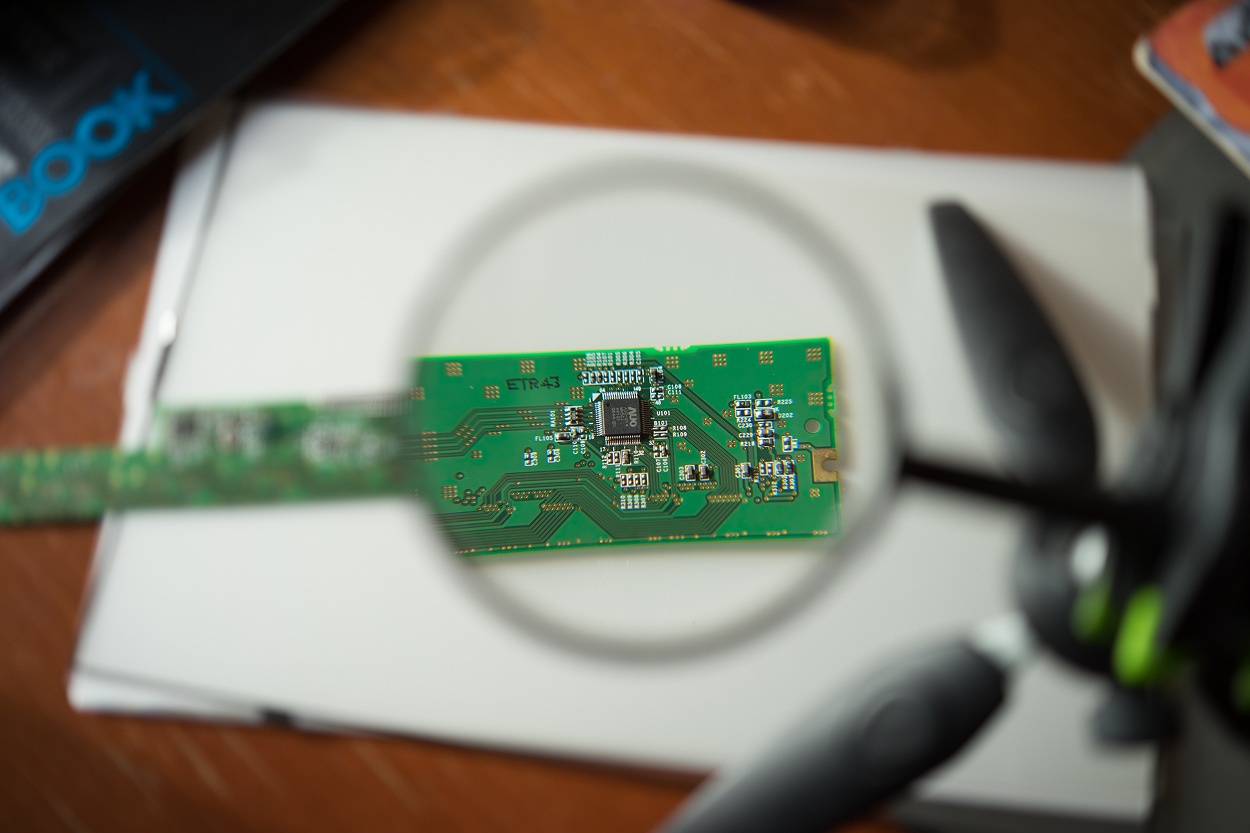
Quick-Turn PCB Fabrication and Assembly in 2026
Quick-turn PCB services have transformed the iteration economics of hardware development. Fabrication and assembly timelines that required weeks a decade ago now take days:
| Service tier | Typical timeline | Conditions |
| 24-hour bare board | 24 hours | Standard 4-layer, DFM-ready Gerbers |
| 48–72 hour turnkey | 2–3 days | Standard components, pre-stocked inventory |
| 5-day assembled prototype | 5 days | Complex designs, sourced components |
| 10-day complex assembly | 7–10 days | HDI, flex-rigid, specialty materials |
AI-driven DFM checks at submission — automated analysis of trace widths, drill-to-copper clearances, solder mask openings, and panelization — eliminate the back-and-forth between designer and fabricator that historically added days to each iteration. Fabricators including JLCPCB have deployed self-developed CAM software for 2/2 mil trace/spacing precision with real-time component inventory synchronization across more than 200,000 parts and algorithmic panelization for yield optimization.
For complex designs that cannot use fast-turn commodity services — HDI with blind and buried vias, flex-rigid combinations, or tight impedance-controlled stackups — the timeline is longer but the DFM-first principle still applies. Submitting DFM-complete files to a specialized fabricator eliminates the review iteration cycle that is the primary source of delay in complex builds.
The rule is: the prototype's job is to test a specific hypothesis, not to demonstrate a finished product. Minimum necessary hardware for the experiment reduces cost, reduces fabrication complexity, and enables faster iteration.
Digital Twins in Hardware Prototyping — 2026 State
Digital twin technology applied to electronics prototyping has matured from a research tool to a practical engineering workflow. The Synopsys Electronics Digital Twin platform launched in March 2026 demonstrated the direction: cloud-native virtual prototyping that enables up to 90% of software validation before physical hardware is available, with pre-integrated tools for automotive SoC and ECU development.
For embedded product development broadly, digital twin applications during prototyping fall into three categories:
Virtual hardware-software integration allows firmware development and system-level testing to begin before physical prototypes are built. Virtual ECUs, simulated sensor interfaces, and emulated peripheral behavior allow the firmware team to execute the full software stack in a validated virtual environment. When physical hardware arrives, the integration work is largely complete.
Thermal and mechanical simulation identifies design risks before physical build. CFD-based thermal simulation predicts junction temperatures under load conditions that match the product's use environment. FEA-based mechanical simulation validates enclosure structural integrity and connector retention force. Both are significantly cheaper to correct in simulation than in a fabricated prototype.
EMC pre-simulation identifies layout-level sources of radiated emissions before the first board is submitted for fabrication. AI-assisted layout analysis tools identify return path discontinuities, poorly routed high-frequency nets, and decoupling placement issues that are likely to cause EMC failures. Correcting these during layout costs hours; correcting them after a failed EMC pre-scan costs a board spin.
Digital twins typically yield ROI within 12–36 months in manufacturing deployments, with some applications returning value within 3–6 months. For product development applications, the ROI is more immediate — each avoided board spin at $5,000–$30,000 NRE plus 2–4 weeks schedule is a direct return on the simulation investment.
The Prototype-to-Production Transition
The transition from validated prototype to production-ready design is a structured process with specific deliverables at each gate. Many programs treat this as a documentation exercise rather than an engineering activity — the result is manufacturing problems that the documentation failed to capture.
The transition requires completing four parallel workstreams before production authorization:
DFM and DFT final review with the EMS partner verifies that the design as-built at prototype can be manufactured at volume using the specific equipment and process capabilities of the production facility. This is not the same as generic DFM analysis — it is facility-specific review that applies the EMS partner's actual process constraints to the current design revision.
This is where many prototype programs fail: the design is technically validated, but the production path has not been checked against BOM substitution risks, EMS process limits, and test coverage requirements. A structured prototype-to-production transition and EMS readiness review helps identify these risks before they turn into field returns after the first production batch.
BOM rationalization ensures that every component in the production BOM has active lifecycle status, available inventory, and at least one qualified alternate. Prototype BOMs are typically not rationalized — they use whatever components are available. Production BOMs must be structured for long-term supply.
Complete manufacturing documentation package — fabrication files at current revision, BOM with approved alternates, assembly drawings, test procedures, firmware images, workmanship standards — is prepared and validated against the current prototype before handoff to EMS.
Pilot build with defined exit criteria validates that the EMS can build the product to specification at production process parameters. Exit criteria — first-pass yield targets, defined acceptance thresholds, zero open critical defects — are established before the pilot begins.

Rapid Prototyping Toolchain Summary
| Category | Tool/Platform | Primary use in prototyping |
| Schematic and PCB | Altium Designer, KiCad, Cadence OrCAD | Layout, DFM check, gerber generation |
| Mechanical design | SolidWorks, Fusion 360 | Enclosure co-design, STEP/IDF exchange |
| Thermal simulation | SimScale, Ansys Icepak | Junction temperature prediction pre-build |
| EMC simulation | Ansys HFSS, Altium PDN Analyzer | Radiated emission risk before fabrication |
| Electronics digital twin | Synopsys eDT Platform, Cadence Palladium | Software validation before hardware |
| Firmware development | Zephyr RTOS, PlatformIO, ESP-IDF | Concurrent firmware on eval boards |
| Quick-turn fabrication | JLCPCB, PCBWay, MacroFab, Proto-Electronics | 24–72 hour prototype builds |
| Component intelligence | Octopart, SiliconExpert | BOM lifecycle and availability check |
Quick Overview
Key Applications: proof-of-concept validation for new electronics products, EVT and DVT builds for complex embedded systems, IoT gateway and industrial sensor prototyping, wearable and medical device hardware development, automotive ECU pre-silicon firmware validation
Benefits: 48–72 hour quick-turn PCB assembly enables daily iteration cycles; digital twin simulation identifies thermal and EMC risks before physical build; parallel hardware-firmware development compresses elapsed time; DFM review during layout avoids board spins averaging $5,000–$30,000 each; 90% software validation before hardware availability achievable with electronics digital twin platforms
Challenges: quick-turn services are limited to standard stackups — HDI and flex-rigid require longer cycles; digital twin setup requires investment in simulation models and virtual hardware; parallel development requires explicit interface definition before streams can separate; prototype-to-production transition is a structured process, not a documentation handoff
Outlook: AI-driven DFM analysis integrated into EDA tools providing real-time layout feedback; electronics digital twin platforms enabling shift-left software development across automotive and industrial applications; quick-turn PCB market growing at 7–9% CAGR; AI-powered visual inspection raising prototype assembly yields above 93%; HDI and flex-rigid boards expanding design possibilities for wearable and medical applications
Related Terms: rapid prototyping, quick-turn PCB, EVT, DVT, DFM, DFT, digital twin, electronics digital twin, hardware abstraction layer, SIL, HIL, thermal simulation, EMC pre-scan, board spin, NPI, pilot build, JLCPCB, Synopsys eDT Platform, Altium Designer, KiCad, STEP/IDF, Zephyr RTOS, parallel development
Our Case Studies in Electronics Manufacturing


FAQ
What is the difference between a proof of concept, EVT, and DVT in hardware development?
How much does a PCB board spin cost and how can it be reduced?
How can digital twins accelerate firmware development before hardware is available?
What documentation is required for a prototype-to-production transition?