The Art of FPGA Debugging: How to Speed It up With Smart Design & Testing Tricks
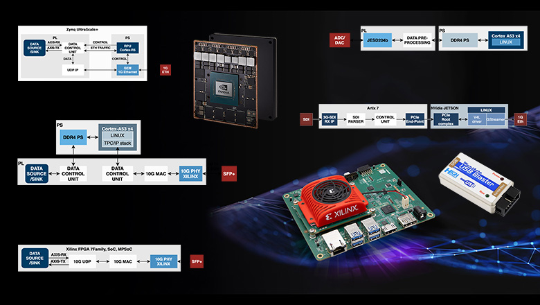
Examples of FPGA projects based on Nvidia Jetson, Zynq UltraScale+, and Xilinx KRIA
Let's try to optimize the most time-consuming stage of electronics design based on FPGA — we mean the FPGA firmware debugging. This article will talk about the 20/80 principle for the planning FPGA design project, consider debugging tools, recall Gordon Moore and Winston Churchill (yes, they have something to do with it). Also, we will touch on debugging of complex distributed FPGA systems with external interfaces and, finally, deal with typical mistakes and best engineering practices.
Contents
- Intoduction
- The 20/80 principle for the FPGA design and debugging project
- FPGA debugging tools
- Debugging distributed FPGA systems
- Challenges of debugging distributed systems
-
First, let's look at a usual FPGA design project:
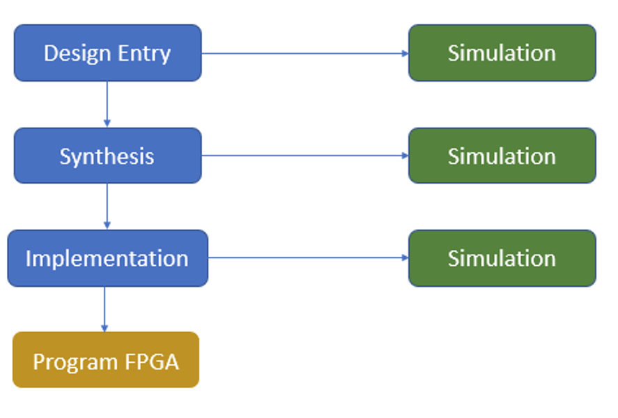
- FPGA programming using standard blocks + actual development of one or two specific blocks.
- Simulation for checking the basic functionality of our device.
- Synthesis.
- Implementation.
- FPGA firmware.
- Testing that frequently turns into debugging.
After each of the first three stages, including synthesis, the classical development cycle includes a simulation stage.
In practice, modeling a synthesized project is actually a check to ensure that our synthesizer is working correctly, so we cannot discover anything new for us at this stage. In general, the result of the behavioral simulation should not differ from the simulation after the synthesis stage if the synthesizer properly understands our code written in one of the hardware description languages (HDLs).
Post-implementation simulation will check whether the design performs the given function with respect to real timings and layout inside the crystal. If you spend enough time modeling the RTL description, you can save time in the debugging phase.
The 20/80 principle for the FPGA design and debugging project
Our experience and that of our colleagues show that modeling and debugging take up most of an FPGA project's timing. You can focus on Pareto's law: about 20% of the time is spent on the development itself, writing code, implementing the upper-level design in the form of a block diagram, and about 80% is used for testing, debugging, and support.
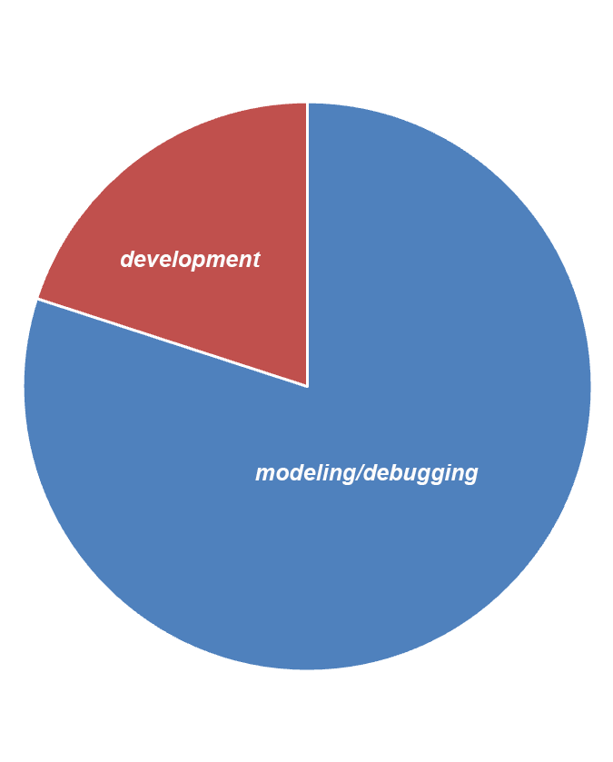
Diagram "Distribution of time to develop and debug an FPGA project"
Why do we have this kind of 20/80 ratio?
- This is partly due to the iterative development process itself. Each iteration takes a long time, and large projects take a long time to assemble. For example, an hour and a half is a required minimum for the typical Xilinx FPGA project (such as Xilinx Zynq UltraScale+). There are larger projects that can take much longer to assemble.
- To complete the debugging process, a software engineer needs not only the skill of FPGA programming in one of the hardware description languages (HDLs or create its block design) but also programming skills in other languages. For example, C and Python for writing some test scripts. You may also need a scripting language such as Tcl.
Now let's look at how to shorten the debugging phase, which is the last one in our workflow but takes up the bulk of the project's time.
FPGA debugging tools
High-level or embedded software engineers have an extensive toolkit: debuggers, the ability to execute program code step-by-step, and extensive program logging capabilities. As for FPGA engineers, they have a limited set of tools to debug their FPGAs. So, what do we have:
- Measuring equipment: oscilloscopes and logic analyzers. These tools allow you to understand what's going on outside your FPGA, but they don't let you look inside it. You can use them to debug the external interface and see how the FPGA interacts with the outside world.
- Built-in debugging tools enable you to look inside your FPGA. All popular FPGA manufacturers have such tools with different names: Xilinx, the most popular manufacturer, offers ChipScope, Intel(ex. Altera) has SignalTap, Microchip (ex. Microsemi) uses a product by Synopsys, which is called Identify RTL Debugger. These built-in debuggers are similar in function.
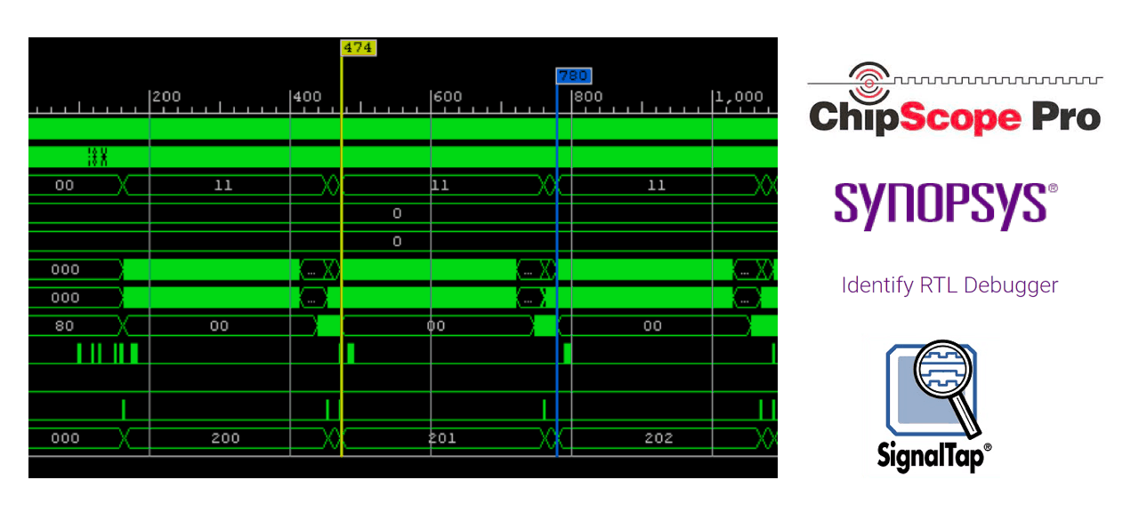
Examples of embedded debuggers from Xilinx, Intel (ex. Altera) and Microchip (ex. Microsemi)
Limitations of built-in debuggers
A destructive control method
When using built-in debuggers, it is essential to remember that ChipScope, SignalTap, and Identify RTL Debugger is a destructive control method. When we add a debugger inside the FPGA firmware, we break its logic:
- We take up some of the FPGA's resources, which changes the project's layout inside the chip.
- We change the timing.
- As a result, we get a different product than before using ChipScop or other built-in debuggers.
'Samples vs. Signals' dilemma
The built-in debugger uses FPGA resources for its work — such as memory resources — so we are faced with a choice: to view many samples and few signals OR to view a lot of samples but a reduced number of reports. The FPGA software engineer has to choose samples or signals. We have to determine the optimal set of observed signals and the optimal observation time.
A simple example: we want to view 4096 samples at 200 MHz, which is only 20 µs of real time. And within 20 µs of real time, you can sometimes see a part of the process you're trying to debug. And if we want to observe a pair of 512-bit buses, that would require 4 Mbits of FPGA memory, which is a large percentage of the available memory in some chips.
Step-by-step execution
This interesting feature is available in the Synopsys debugger for Microchip (ex. Microsemi) FPGAs only — we mean the so-called step-by-step execution, a usual thing for engineers developing high-level software. This feature is announced as a progressive solution, although the debugger itself is far from new.
The Synopsys debugger allows you to stop executing your FPGA firmware at a certain point and continue to run the code clock cycle by clock cycle. An attractive solution, but in this case, a debugged project will have a lot of limitations:
- In practice, the step-by-step execution helps you debug a project consisting of a single synchronization domain. This function will be irrelevant to larger FPGA projects.
- If the project has external interfaces bound to real-time (even the most trivial UART), then we break all communication with external devices at the moment of stopping the execution. After one such stop, further step-by-step execution makes no sense.
Conclusion: It is an interesting tool, but we have not yet been able to find a good use for it in practice.
Moore, Churchill, and the rules of FPGA debugging
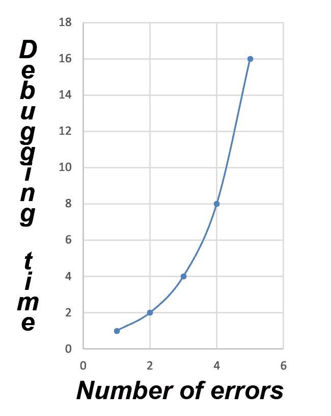
Before we go any further, we want to share with you two valuable rules to plan the FPGA debugging phase and not get discouraged in the process. :-) The first rule of thumb sounds like Moore's Law: "It will take twice as long to find each successive error than the previous one." This information helps to estimate FPGA debugging time adequately.
What is the reason for such an increase in time consumption? Each successive error occurs under much more difficult initial conditions, and it takes much longer to repeat those conditions. Our experience shows that this principle works: if you look for the first mistake within a day, the following error would require at least two days.
The second rule of thumb is a modified statement credited to Winston Churchill. He said that success is the ability to go from one failure to another with no loss of enthusiasm.
«For an FPGA engineer, debugging is about going from one error to another without losing enthusiasm.»
The last part of the statement about enthusiasm is the most important because FPGA debugging feels like a constant emotional struggle with the firmware. After each of your wins, the firmware sort of says: "No, my friend, don't relax, stay tuned, I have one more error for you, and it will take you twice as long to find it."
Debugging distributed FPGA systems
When debugging simple systems with one board and one FPGA, there are some challenges, but they are manageable. And debugging of complex distributed systems is another matter entirely. By distributed systems, we mean two types of them: heterogeneous and homogeneous ones.
For heterogeneous systems, the debugging rules are about the same: each board performs its function; we debug each one individually, and then all together as a system.
Here is an example with homogeneous systems: we have a VPX module with 12 slots. Let's assume that there are ten slots with FPGA, one slot with a PCI Express switch, and one slot with a CPU that aggregates all this data, processes it, and passes it on. Such a system is homogeneous in structure because each module performs the same function.
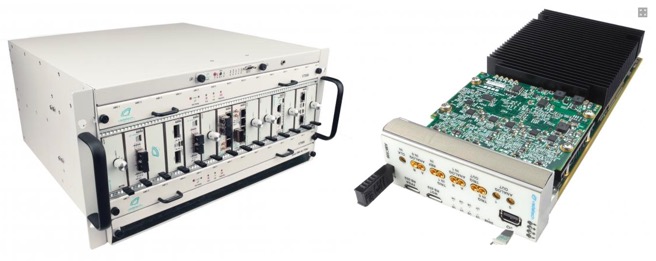
The photo on the left shows the VPX system with 12 slots; on the right is the FPGA module that will be inserted into it
When debugging homogeneous systems, we are faced with a scaling effect: if we debug one board, run all the tests, and make sure that it works, then the scaling effect does not guarantee that the system will work that way on two boards. When we have debugged the system on two boards, it does not guarantee that all three boards will work that way, and so on — until we make the system work correctly on the whole array of our boards.
Challenges of debugging distributed systems
1. Inability to connect to all FPGAs simultaneously. If we have a large number of FPGA devices, we cannot connect them to our built-in debugger via JTAG at the same time. The first problem: you may not have ten computers to connect to each module. The second problem is common to VPX systems, where FPGA devices are connected to the same JTAG chain, and therefore you just cannot connect to all of the FPGAs simultaneously.
2. The non-deterministic nature of error events, i.e., an error can equally likely occur in any of 10 or N modules. It significantly complicates the debugging process. Firstly, you must repeat the situation that caused the error. Secondly, we have to use the built-in debugger on the board where we hope to see the error, i.e., here we have no tools except luck and multiple test runs until the error appears where we expect it to be.
3. The complex error detection criterion is the third difficulty we encounter when debugging complex distributed FPGA systems and beyond. Often an error cannot be detected inside an FPGA (from the FPGA's point of view, the data are correct), but when we pass this data on to a signal processor, it can detect an error in it. Even if it informs our FPGA about it with some feedback signals (we can run a built-in debugger at this moment), we will not see this error because the event occurred long ago on the timeline in the past, and we can not determine the cause of the error.
What should we do? In this case, when debugging, you can add additional blocks inside the main device that control the input data. Sometimes, the complexity of these control blocks can be comparable to the complexity of the blocks we develop to implement into our FPGA project.
Debugging external interfaces
Every FPGA device interacts with the outside world in one way or another, so we can't avoid debugging external interfaces.
FPGA firmware blocks interact with each other and with third-party devices because if a block has no external links, then at the stage of synthesis, it will be removed from the project for its optimization.
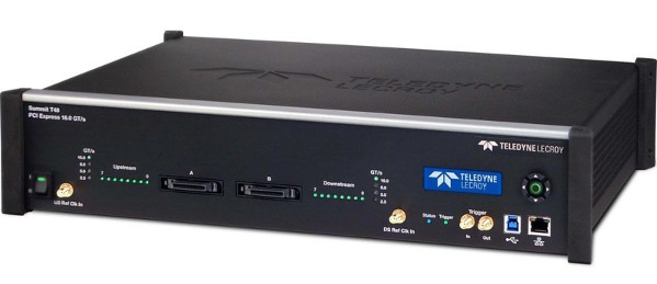
LeCroy PCIe protocol analyzer (expensive equipment that makes debugging a lot easier)
Block design implies that blocks interact via standard interfaces: Xilinx has AXI Memory Mapped and AXI Stream, Intel FPGA has similar interfaces — Avalon MM and Avalon Stream. Also, engineers use the standard APB bus. In terms of debugging, these are pretty simple interfaces with a limited number of states and control signals, so there should be no serious problems. Moreover, some manufacturers have ready-made solutions for it. For example, Xilinx has specialized units that allow you to check the correctness of the protocol on the fly and detect errors on your bus. Thanks to such a block, you can fix the error moment and then use a built-in debugger to find out what caused it.
This is not the case when one of the interfaces is used as a transport for a higher-level protocol. For example, let's take a low-level PCI Express core that operates at the TLP packet level and uses the AXI Streaming interface as its transport to transmit these packets. AXI Stream is a standard interface; we understand how it works, but we have no way to debug it and monitor the correct formation of TLP packets that we pass through AXI Stream to the PCI Express core.
When programming and debugging such blocks, an FPGA software engineer faces problems that cannot be resolved without expensive specialized equipment. For PCI Express, this would be a PCI Express protocol analyzer—without such equipment, debugging means working with a black box. The maximum that is available to you is a compliance check for the AXI Stream interface.
Therefore, if a project involves working with interfaces such as PCI Express, 10/100G Ethernet, or more specific ones such as Infiniband, you will have to consider that the debugging stage will require good analyzers, which will significantly simplify the work process. As a result, the same PCI Express controller will no longer be a black box because you will be able to analyze the behavior of the PCIe bus.
If we do not have access to special equipment for analysis and debugging, you can use behavioral models—for example, a model for the PCI Express controller. However, such a model will only be able to cover a small amount of all the possible situations that your FPGA device can encounter in real life. If you try to provide a higher percentage of coverage, the simulation may take indefinitely, and the project will not be completed.
So here are three challanges that FPGA software developers face when debugging their external interfaces:
- Unable to adjust external interfaces
- The need to use expensive equipment for debugging:
- PCIe and 10/100G Ethernet analyzers
- 10-25 Gb/s oscilloscopes with traffic analysis function
- Black box models will not cover 100% functionality, especially in the real-time part
Three common mistakes of the FPGA debugging process
Now let's look at the typical mistakes at the debugging stage. If you manage to avoid them, you will save a lot of time on your FPGA design project.
Mistake #1. Making two or more corrections in one assembly
Given that building a project can take several hours (or even a day), there is a temptation to fix several bugs noticed at once. But as practice shows, especially with complex projects, an attempt to make two or more fixes at a time often leads to even more unpredictable behavior of the debugged FPGA system (than it was before making the fixes). This is because of the complex logical connectivity — both between and within blocks. As a result, you have to go back and check one correction after another.
The solution to this problem is quite simple: despite a long time it takes to rebuild the project, you should move step by step. One fix, then build and check, the next fix should be followed by a new build and second check again, and so on. This way, you save more time and effort.
Mistake #2. False confidence in the correctness of your algorithm and performance of your block based on code analysis
How does this happen? FPGA software engineers look at their code, understand how it should run, and don't even try to add a built-in debugger to see what's going on there because "well, it's obvious from the code that everything should work fine."
Let's take a classic error: different bus sizes. If you try to compare two signals of varying digit capacity in a logical operator such as "if" in VHDL, then in terms of syntax and visually, everything will look fine. Still, the synthesizer will convert this comparison to eternal false, and, accordingly, the algorithm will not work.
We encounter a similar error in the Verilog language, where you can freely assign one signal to another without controlling the digit capacity. Suppose we assign a signal of higher digit capacity to a signal of lower digit capacity. In that case, we will lose some significant bits. However, the code analysis will perceive it as a correctly written logical condition in the first case and no less correct signal assignment in the second case.
The solution: when debugging, if possible (and memory resources allow), you should output to your debugger all the signals that are somehow involved in your logical condition because even obvious things can lead to incorrect block behavior.
Mistake #3. Shifting your problem to a colleague unit or external chips
This can be done not only by beginners but also by experienced engineers, assuming that errors occur not in their code but in the block of their colleague or even in a standard core or external chip, exchanging data with an FPGA.
We must admit that errors occur in standard units and even in mass-produced chips, and most of them are documented.
The solution: even though there may be an error even in a standard Xilinx core, we have to follow the "presumption of guilt" and assume that an error did occur in our block and not in a standard IP core (for example, AXI4 Interconnect, which for some reason blocked our transaction). Of course, your extra letter to the technical support service of your vendor will not be out of place.
Practical recommendations
Finally, let's look at the following list of eight practical recommendations to make the FPGA programming process more or less manageable.
1. Error counters. Add them wherever possible. Checksum errors, access errors, protocol errors. For example, we see a CRC error — we start the CRC error counter. If we notice any invalid data in some package — we take them into account, too.
2. Statistics counters: data counters, packet counters, request counters. All blocks process data in one way or another — as input or output. It is helpful to put a counter to see how much we got on input and how much data was passed to the output. If it is packet data, then count the number of packets. If packets are preceded by some request (handshake) — count these handshakes. In the debugging phase, counters will help you determine where data is lost in a long chain of several blocks.Providing access to FSM states The sixth recommendation concerns another vital element of FPGA digital circuitry - finite state machines. They allow you to describe the logic of your device in the most visual form, such as packet parsers, AXI MM interface controllers, and more. Access to machine states allows you to understand in which state the device is freezing and what signal it is waiting for to go from one state to another.
3. Detecting "impossible" states and situations. Why is an impossibility used in quotes? Because nothing is impossible in the fascinating world of FPGA. :-) Any situation can arise, and you should always be ready for it, i.e., detect it. Let it be a flag showing that your device was in a state that is not in the specification. And, when we get a ready-made FPGA device with sudden freezes, these flags will show us that this situation did occur in the past and needs to be processed correctly.
4. Processing of all error signals. If error signals come to your unit from third-party units or interfaces, they must be processed, even if they seem unlikely or impossible. At least, all error signals should be recorded in order to determine the cause of the problem when the device stops working or its behavior becomes unpredictable.
Let's go back to our PCI Express controller for an example: why should we process such an error such as link loss? The probability that an endpoint that communicates with the root complex suddenly loses the link tends to be zero, but we should know that it happened in the past if such a situation occurs.
5. Analysis of FULL / EMPTY flags and UNDERFLOW / OVERFLOW situations.
This recommendation applies to everyone's favorite component of the FPGA world — FIFO (first in, first out). It is an essential element of digital circuitry used to transfer data from one synchronization domain to another, to smooth out the speed difference between a receiver and a transmitter, and for its direct purpose — buffering.
For debugging, it is useful to add logic that will detect situations of reading from an empty buffer (underflow) and writing to the overflow one. So we will quickly find the place where data is lost, or, conversely — where they appear out of nowhere.
The sixth recommendation concerns another vital element of FPGA digital circuitry - finite state machines. They allow you to describe the logic of your device in the most visual form, such as packet parsers, AXI MM interface controllers, and more. Access to machine states allows you to understand in which state the device is freezing and what signal it is waiting for to go from one state to another.
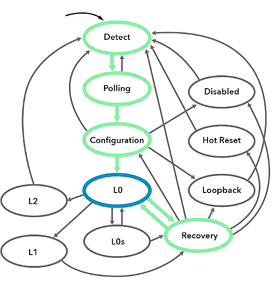
LTSSM — link training and status state machine
The finite-state machine (FSM) shown in this diagram is a PCI express link initialization machine (LTSSM). Almost all PCIe cores allow bringing the state of the FSM outside of the core — even major vendors, such as Xilinx and Altera, make use of this requirement.
7. Read the documentation from cover to cover
It may be a boring thing to do but a beneficial one. If an interface or IP core you are working with has documentation (and it should), read it in its entirety. Yes, this piece of advice may seem strange because some cores haНve documentation with a hundred or more pages. It will take some time to read it, but you will probably save a lot more time because even the standard interfaces used in certain cores do not always work as expected.
For example, let's take the PCI Express core working at the TLP packet level. You read the documentation and see that AXI Stream is used for interacting with a user. You are tempted to flip through this part, because you already know how the AXI Stream interface signals work and what they are responsible for. But as for the PCIe core, its hand-shake logic is different from the AXI Stream standard (in Xilinx FPGAs in particular). If you don't take this into account, it can take a very long time to find an error, especially if you don't know where to look for it.
8. Use automatic synthesizers, such as HLS and Simulink (where possible)
Finally, here is our last piece of advice: do use automatic synthesizers whenever possible. For example, the HLS environment that allows you to implement your logic in C / C++. Or the Simulink product that enables you to implement FPGA logic based on a vast set of standard library components, and then with a click of a button, synthesize HDL code from this description. Yes, this code will be unreadable from the point of view of FPGA firmware developers. Obviously, the code written in HLS or implemented in Simulink requires high-level behavioral verification and modeling. Still, you can be sure that the generated HDL code, despite its unreadability, will work in your FPGA.
In conclusion, we would like to note an important aspect: the recommendation to "provide access" to various counters and states within your FPGA can be implemented in several ways:
- You can add a built-in debugger, such as Chipscope, to the variables you set. But sometimes, there are too many of these signals, and leaving the Chipscope in your FPGA device that you will hand over to your customer for industrial implementation and testing is not quite right.
- Provide access through one of the available interfaces to all registers that you can start at the code description stage. Examples of implementation:
- Mapping registers to the address space of your device if it communicates with the outside world, e.g., via PCI Express.
- Providing access via the most robust interface possible. For instance, via UART.
- Remember our favorite LEDs: there is no better way to indicate the performance of your device with the developed FPGA firmware onboard.
Of course, it's impossible to talk about all the intricacies of FPGA debugging in this article; that is why we used the word "art" in its title. Each situation requires a meaningful approach and a specific debugging method. So if you want to get to the bottom of your particular situation, feel free to write to us here on the contact page or on social media.
Our projects


