In-Mold Electronics (IME): How It Works and Why It’s a New Trend
For several years now, electronics manufacturers have been discussing a breakthrough technology that will change the devices we use and the approach to their design: no more mechanical buttons and switches, reduction in thickness to 2 mm, about 70% lighter, and 30% cheaper.
We are not talking about future mass-produced devices like the double folding and rollable screens recently showcased by Samsung, but about the production technology already used in industrial and automotive electronics, home appliances, IoT, and wearable gadgets. This technology is called in-mold electronics or IME. Unfortunately, we haven't yet written about this exciting topic on our blog. So, let's fix it.
Contents
- Introduction
- What is the difference between in-mold decoration (IMD) and in-mold labeling (IML)?
- Wrapping up
We are starting with a spoiler and note right away that IME is not something radically new but an evolution of technology that we used before. With the emergence of more stretchable materials and better conductive inks that can withstand molding at high temperatures, engineers could do without rigid printed circuit boards in some projects and apply conductive tracks directly to plastic surfaces of electronic devices. As a result, we can get rid of the 2D flat electronics and switch to flexible PCBs and 3D structural electronics with resistors, integrated circuits, sensors, antennas, and LEDs that cover the curved surfaces.
Now let's go over everything in order. In-mold integration of electronics is a type of in-mold decoration (IMD). With IMD, enclosures for electronic devices are decorated under pressure directly in molds or in the process of blow molding. The result is a ready-made part that does not require additional surface treatment, marking, or painting.
The principle of In-Mold Labeling (IML). Image credit: Maspi S.r.l.
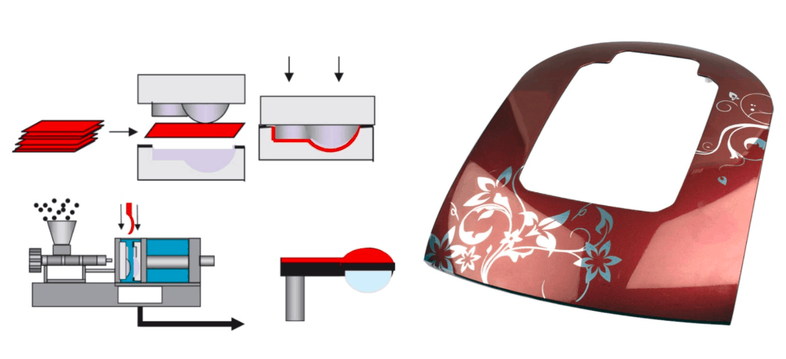
The picture above shows the main idea of the IMD and IML technologies:
- First, the desired pattern — text, decor, or texture (e.g., a company logo or button captions) — is applied to a thin film plastic. This is done through the screen or digital printing. As a result, we get so-called "in-mold appliqués."
- The appliqué is placed in a mold tool.
- Then dry polymer pellets are poured into a molding machine; they are melted and pressurized into the mold — behind or ahead of the film.
- The form is filled with polymer, and the printed label is "glued" to the plastic enclosure.
- At the output, when we open the mold, we get a ready-made part of the plastic enclosure with integrated graphics.
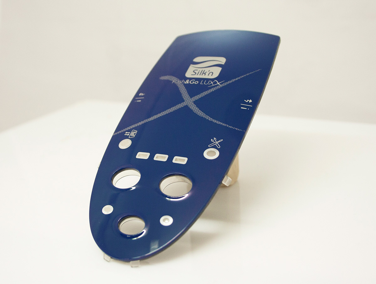
The photo above shows the top panel of the remote control, made with in-mold decoration (IMD). You are undoubtedly familiar with other examples of devices made with this technology: multimeters, automotive dashboards, toys, and mobile phones.
What is the difference between in-mold decoration (IMD) and in-mold labeling (IML)?
If graphic or texture inside the mold is not applied to the entire surface of the enclosure — from edge to edge — but on a separate area, this type of decoration is called "in-mold labeling" or IML. With this technology, you can add color, graphics, and textured areas.
IML is often used to add logos, warning signs, certificate icons, part numbers, or short instructions. You've probably seen these labels on disposable packaging and plastic containers for home use.
And now we're back with in-mold electronics, which was a logical continuation of the previous two technologies. It looks like the first commercial implementation of IME was realized in an innovative overhead console for a Ford car in 2012. Today, IME is used for household appliances, automotive dashboards, medical equipment, aerospace, and wearable electronics.
This technology combines a decorative application of the IMD process with fully functional electronics. But in this case, the film is not printed with decor or text but with conductor tracks made of conductive silver inks; you can also mount resistors, microcircuits, and LEDs to the film.
The molding process results in plastic parts with thin walls (up to 2 mm) of sufficient durability, high functionality, with pre-integrated lighting, keypads, and decorative elements.
The image below shows how this works:
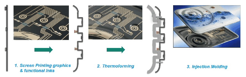
Image source: Functional Ink Systems for “In Mold Electronics” by DuPont
- Screen printing of graphics and conductive tracks with functional inks on thin polyester or polycarbonate film.
- Thermoforming gives printed media a three-dimensional shape that matches the injection mold.
- Injection molding.
IMEs are usually thermoformed, but not always. For example, in areas with a touch screen interface, the surface may remain flat.
An emerging trend is the use of polyethylene terephthalate (PET), which does not mold well but is suitable for designs with a smaller radius of curvature. However, PET does not tolerate high heat, so so the electronics market now needs low-temperature solders.
While consumers still perceive this technology as innovative, the conductor tracks look like decorative elements. :-) In time, industrial designers and hardware startups will surely come up with fresh ideas on how to use the possibilities of this type of molding.
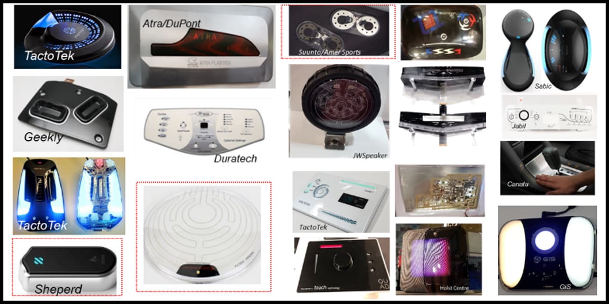
Image source: analyst report by IDTechEx, 2020.
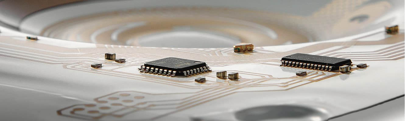
The photo above shows serial devices and prototypes created with in-mold electronics. Also, you can see the IME devices in new cars and home appliances, where the shape of the electronics matches the curved forms of envisioned designs.
Capacitive touch control and user interfaces
The capacitive touch technology is used in many IME applications. This interface replaces pressing a physical button with the touch of a finger. The tracks on the circuit board are located under the touchpoint and monitor the change in the electrostatic field. When we touch a capacitive panel, a small charge is drawn to the point of contact, and our finger acts as a functional capacitor. For example, in a car, such interfaces are used to turn on the headlights, power, or adjust the volume.
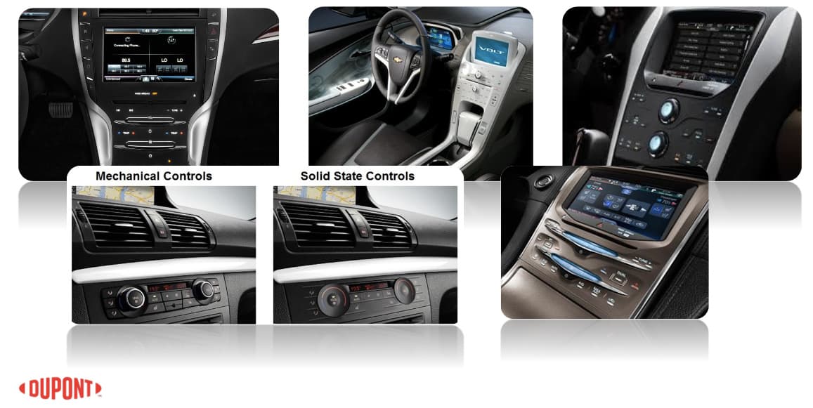
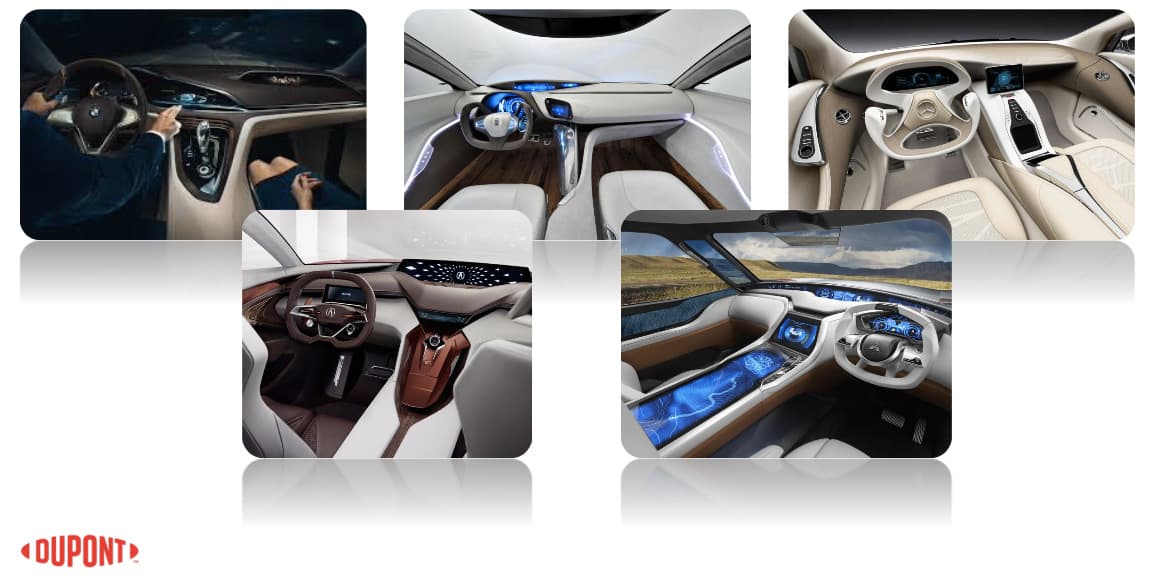
Here's how the American chemical company Dupont, one of the world's developers of conductive inks for IMEs, is presenting interfaces for cars of the present and future:
Wrapping up
The automotive industry is just one of the many applications of IME we've already mentioned above. We will use this field for a case study to illustrate the subject of this article. Let's take the overhead console in a car, which was designed with a printed circuit board and a plastic enclosure, consisting of dozens of prefabricated parts, and compare it with the console of the Finnish company TactoTek, which is now developing its IMSE technology or so-called in-mold structural electronics:
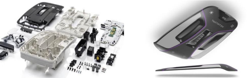
Image source: Functional Ink Systems for "In Mold Electronics" by DuPont
| Standart design | IME Design | Difference | |
|---|---|---|---|
| Weight | 650 g | 150 g | −77% |
| Thickness | 45 mm | 3 mm (flat version) | −93% |
| Mechanical parts | 64 pcs. | 2 pcs. | −96% |
| PCBA size | 10 x 4 sm | 10 x 3 sm | −25% |
As you see, there is a significant reduction in weight, size, the number of moving parts, and, as a consequence, the reliability and cost of the device as a whole. Judging by the current development of this technology and analysts' reports, predicting an increase in IME implementations from 2023−2024, a new trend is looming in the electronics market. We will see a transition from flat and rigid printed circuit boards inside a box-shaped enclosure to three-dimensional structured electronics.
So if your work is related to hardware design and electronics products, you can look closely at this opportunity and have time to get on the crest of the wave. As for the Promwad engineering team, we hope that we will soon be able to share our case studies on the design and production launch of in-mold electronics.
Our projects