Next-Gen PCB Design for High-Speed Interfaces: PCIe Gen5, DDR5 & Beyond
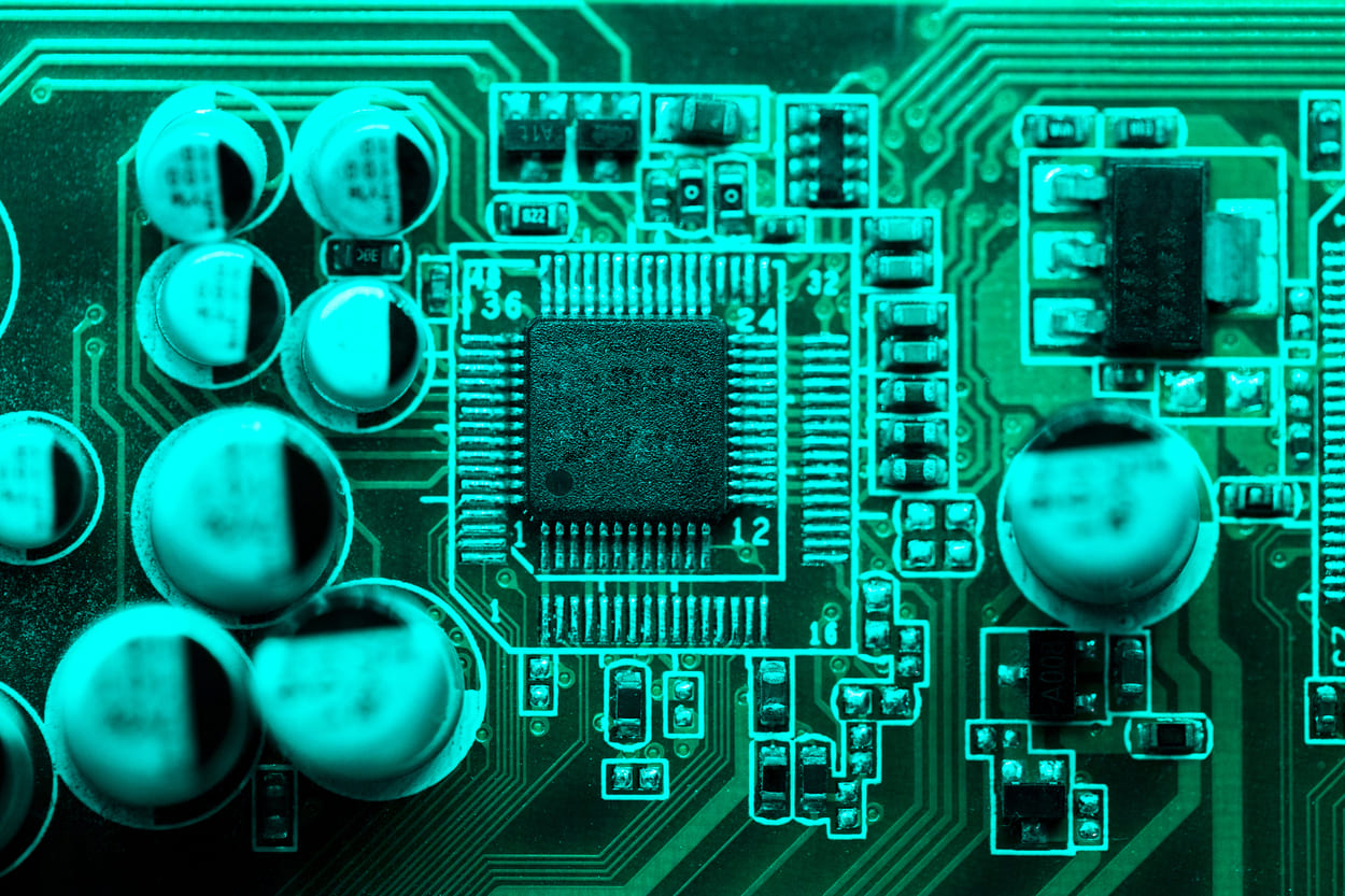
As modern electronic systems demand ever-increasing data rates, the complexity of printed circuit board (PCB) design rises accordingly. High-speed interfaces like PCIe Gen5 (32 GT/s), DDR5 (up to 6400 MT/s), USB4 (40 Gbps), and 10G+ Ethernet place immense stress on signal integrity, power delivery, and thermal management. Designing for these protocols requires specialized knowledge, tools, and methodologies to ensure reliable operation.
In this article, we explore how engineering teams approach next-gen PCB design, the common pitfalls to avoid, and how Promwad helps clients bring their high-speed systems to life.
Why High-Speed Interfaces Matter
Applications in automotive, telecom, data centers, and industrial automation increasingly rely on fast, reliable data transfer. The transition from PCIe Gen3/4 to Gen5/6 or from DDR4 to DDR5 offers:
- Increased throughput (e.g., PCIe Gen5 doubles Gen4 bandwidth from 16 GT/s to 32 GT/s)
- Reduced latency for AI, ML, and high-performance computing
- Support for complex sensor fusion and real-time analytics
According to a 2024 Yole Group study, more than 70% of new data center motherboards will feature DDR5 and PCIe Gen5 by the end of 2025.
Key Challenges in High-Speed PCB Design
| Challenge | Description |
| Signal Integrity (SI) | Crosstalk, reflections, and jitter can degrade signal quality. |
| Power Integrity (PI) | Fluctuating current demands require robust power delivery networks (PDN). |
| EMI/EMC | Faster signals generate more electromagnetic emissions, increasing the risk of interference. |
| Tight Timing Margins | DDR5 introduces more stringent timing requirements for data and command signals. |
| Thermal Management | High-speed transceivers and memory require advanced cooling strategies. |
Modern Design Techniques and Tools
To mitigate the above issues, engineers apply:
- Pre-layout simulation: Tools like HyperLynx or Keysight ADS help predict impedance mismatches and SI problems.
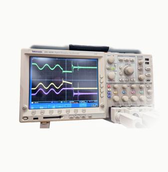
- Post-layout validation: Eye diagram analysis and time-domain reflectometry (TDR) validate trace performance.
- Stackup planning: Controlled impedance requires specific dielectric materials, trace widths, and spacing.
- Via design and back-drilling: Reducing stub length helps minimize signal reflection.
- Differential pair tuning: Crucial for USB4, PCIe, and LVDS to maintain signal fidelity.
Design Standards and Specifications
| Interface | Max Data Rate | Key Constraints |
| PCIe Gen5 | 32 GT/s | Tight skew control, low insertion loss |
| DDR5 | Up to 6400 MT/s | Equalized routing, impedance matching |
| USB4 | 40 Gbps | Minimal return loss, clean transitions |
| 10G/25G Ethernet | 10-25 Gbps | Shielded differential pairs, low crosstalk |
Advanced Materials and Manufacturing Considerations
To support higher frequencies and reduce dielectric losses, designers now turn to materials like:
- Rogers 4350B or Megtron6 for high-speed signal layers
- Low-Dk laminates to minimize delay and reflection
- Embedded capacitors and blind/buried vias for compact layouts
Real-World Applications at Promwad
Promwad engineers develop high-speed PCBs for:
- Custom networking equipment (Ethernet, fiber, TSN)
- AI/ML edge computing modules with PCIe Gen5 and DDR5
- High-throughput video processing boards (USB4, HDMI 2.1)
- Automotive ECUs for autonomous driving and ADAS
In one project, our team designed a multi-layer board supporting DDR5 memory and PCIe Gen5 links with under 2% insertion loss and full compliance with signal integrity specs.
Design Tips for Engineers
- Use serpentine routing only as a last resort; try to optimize layer stackup first.
- Always simulate signal behavior across temperature and voltage ranges.
- Maintain reference plane continuity under all high-speed signals.
- Route differential pairs with matched lengths and spacing.
- Collaborate closely with your PCB fabricator on via structures and tolerances.
Industry Insights
According to IPC and DesignCon 2024 reports:
- 60% of signal failures in high-speed boards result from poor SI design.
- The adoption of DDR5 and PCIe Gen5 will grow by 35% YoY in enterprise hardware.
- Pre-layout simulation can reduce post-production debug time by 40%.
A LinkedIn poll by Signal Integrity Journal found that 48% of engineers consider "stackup planning" the most critical factor for high-speed PCB success.
In a popular Reddit thread on r/AskElectronics, senior hardware designers cited "via stub resonance" and "poor power decoupling strategy" as top reasons for first-pass failures in high-speed boards.
Conclusion
Designing for PCIe Gen5, DDR5, and other high-speed interfaces is both a challenge and an opportunity. With the right tools, methodologies, and experience, engineering teams can create reliable, high-performance systems that meet the demands of next-generation applications.
Promwad is ready to support clients at every stage of their hardware development journey, from system architecture to layout, simulation, and compliance testing. Reach out to learn how we can help optimize your next high-speed design.

