Reducing Time-to-Market in Electronics Hardware Development: NPI Process, DFM Integration, and Supply Chain Strategy
Hardware development timelines are determined by decisions made early in the design process, not by the pace of assembly at the end. A product that enters manufacturing with unresolved design-for-manufacturing issues will accumulate delays at every subsequent stage — re-spins, sourcing exceptions, test failures, and NPI delays that push volume ramp by weeks or months. The teams that consistently achieve shorter time-to-market do so by front-loading the work that eliminates downstream friction.
The stakes are concrete. The average cost of a PCB design re-spin is $28,000, and avoiding re-spins through early DFM integration is one of the most direct levers for reducing both cost and schedule in electronics development. Beyond direct cost, each re-spin cycle typically adds four to eight weeks of elapsed time — time that compounds with supply chain lead times and EMS onboarding delays.
This article covers the structure of the NPI process for electronics hardware, the specific practices that compress development timelines at each stage, component sourcing strategy in the current supply environment, and the manufacturing-readiness requirements that determine whether a design can be ramped to volume production on schedule.
The NPI Process and Where Time Is Lost
New Product Introduction in electronics hardware follows a defined sequence of validation gates: Engineering Validation Testing (EVT), Design Validation Testing (DVT), Production Validation Testing (PVT), and Mass Production. Each gate has specific entry and exit criteria, and failing to meet them forces a return to the previous stage.
EVT verifies basic functional operation with close-to-final parts. The objective is to confirm that the design works as intended before committing to tooling and production components. DVT validates that the design meets all performance, reliability, and regulatory requirements using production-representative hardware. PVT confirms that the manufacturing process itself — assembly yield, test coverage, documentation — is ready for volume production.
Supply chain volatility, parts shortages, inflationary pressures, and increasing compliance challenges are changing how manufacturers handle NPI. According to Gartner data, only 8% of global supply chains can currently be classified as resilient, and fewer than 6% as antifragile. The most common sources of NPI delay are: design issues discovered at DVT that require a hardware revision; component availability problems that surface after design freeze; EMS onboarding taking longer than planned because manufacturing documentation is incomplete; and test coverage gaps that generate yield problems in PVT. Each of these has a known mitigation — and each mitigation requires work that is often deferred until it becomes a problem.
Design for Manufacturing, Assembly, and Testability
DFM, DFA, and DFT are not separate activities performed at the end of design — they are constraints that must be applied during schematic and layout to avoid downstream problems.
H3: Design for Manufacturing
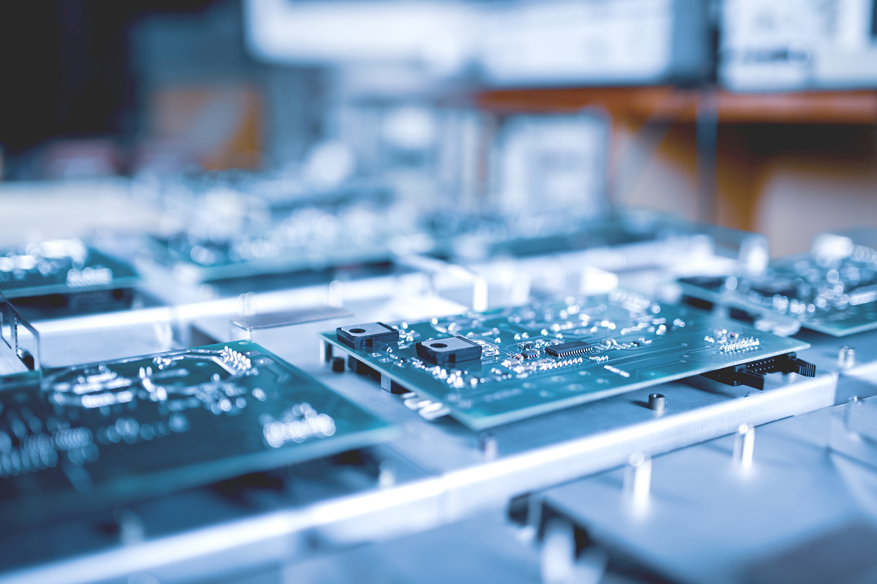
DFM analysis checks that the PCB layout and component selection are compatible with the manufacturing processes of the target EMS facility. Specific checks include minimum trace width and spacing for the fab's capabilities, component clearances for automated placement and soldering, via-in-pad rules relevant to the reflow process, and copper balance requirements that affect board warpage during reflow.
Running DFM checks before finalizing a PCB layout — using tools such as Siemens Valor NPI or EMS-partner-specific review processes — identifies issues when they cost hours to fix rather than days. A DFM finding that surfaces during the first PCB fabrication run requires a board spin; the same finding identified during layout review requires a property change.
EMS partners engaged during the design phase, rather than at design handoff, can provide manufacturing-specific feedback that generic DFM tools do not capture. Different EMS facilities have different equipment capabilities, component library preferences, and process constraints. A design optimized for one EMS may require rework for another.
Design for Testability
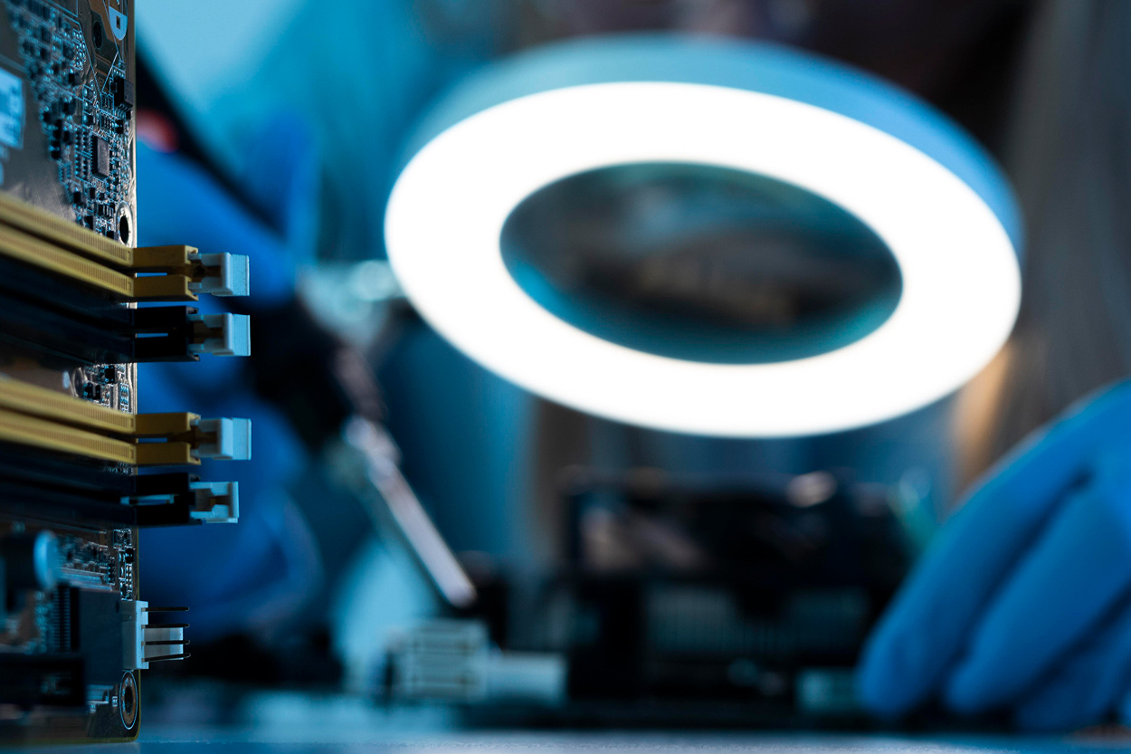
DFT ensures that the assembled board can be verified efficiently at production volumes. The primary requirement is physical accessibility: test points on all signals that need to be exercised, JTAG boundary scan support on complex digital devices, and diagnostic interfaces that allow firmware-level testing without specialized external fixtures.
Boards that lack adequate test point coverage require either manual probing — which is slow and inconsistent at volume — or bed-of-nails fixtures designed around the available access points, increasing fixture complexity and cost. Embedding DFT requirements at the schematic stage costs nothing; retrofitting them onto a production layout is expensive and may not be fully achievable without functional compromise.
Component Selection and Alternate Sourcing
Component selection during design has direct consequences for supply chain risk. Selecting a component available only from a single distributor, approaching end-of-life, or with a manufacturer-quoted lead time of 52 weeks creates a schedule dependency that no amount of NPI process improvement can eliminate.
Lead times for electronic components improved through 2024 following the severe disruptions of 2021–2023, but the improvement is uneven. Long-lead items remain in specific categories, and geopolitical factors continue to create new exposure — particularly in automotive memory, advanced logic, and components using controlled materials. The design-phase mitigations are specific: validate component availability and lifecycle status before committing to a part, identify approved alternates for every critical component before design freeze, and flag any component with a single-source supply or lead time exceeding 16 weeks for procurement attention before the BOM is released to EMS.
Prototyping Strategy
The purpose of early prototyping is to reduce uncertainty, not to demonstrate a finished product. Teams that build fully featured prototypes too early spend time debugging integration issues that could have been identified with targeted experiments — and the time spent is not recoverable.
A more efficient approach sequences prototyping to the actual unknowns. If the critical uncertainty is whether a sensor algorithm works, build a minimum system around that sensor on an evaluation board. If the critical uncertainty is thermal behavior under load, build a thermal test vehicle. Full-system integration comes after individual risks have been characterized.
Parallel hardware and firmware development reduces elapsed time but requires discipline. The firmware team needs a stable hardware target; the hardware team needs firmware to validate functionality. Evaluation boards and pre-production modules give the firmware team a real hardware environment during PCB fabrication, preventing the firmware schedule from waiting on hardware.
3D-printed enclosures are a standard practice for validating form factor, ergonomics, and mechanical assembly before committing to tooling. The cost and lead time of a 3D-printed prototype is a small fraction of injection mold tooling, and discovering an assembly interference or ergonomic problem at this stage avoids a tooling modification that typically costs $3,000–$15,000 and takes two to four weeks.
EMS Partner Selection and Onboarding
The EMS partner is not just a manufacturer — for development-stage hardware, they are an engineering resource. An EMS with NPI experience and engineering capability can provide DFM feedback, validate test strategies, identify sourcing risks in the BOM, and manage the documentation preparation required for a clean production handoff.
Strategically splitting NPI and volume production between locations allows companies to optimize for both speed and cost. Many companies partner with NPI-focused suppliers during development to accelerate time to market, then transition volume production to manufacturers optimized for scale. For EU-based OEMs, EMS facilities in Poland, Czechia, Germany, and the Baltic states combine relevant quality certifications with reduced geopolitical exposure relative to Far East manufacturing.
EMS onboarding — transferring a design from the development team to the manufacturing partner — is consistently underestimated as a schedule activity. Complete manufacturing documentation includes fabrication files, assembly drawings, a full BOM with approved alternates, test specifications, workmanship standards, and acceptance criteria. Incomplete documentation at handoff generates questions and iterations that delay the first build by weeks. Preparing documentation in parallel with prototype validation, rather than after, compresses this stage significantly.
Pilot Build and Production Ramp
A pilot build — typically 50 to 200 units, depending on the product — is the first real-world test of the manufacturing process. It validates that the EMS can build the product to specification at volume, that test fixtures work correctly, that yields are acceptable, and that the production documentation is complete.
Pilot builds consistently surface issues that were not visible in prototype builds: component placement conflicts that only appear when machine-placed at production tolerances, test fixture probe alignment problems, and documentation errors that cause assembly deviations. Identifying these at pilot rather than at volume ramp avoids the cost and schedule impact of stopping a production run.
The key discipline at pilot is to treat it as a process validation, not just a unit production exercise. Each defect found at pilot should generate a root cause analysis and a process correction before volume production starts. Acceptance criteria for exiting pilot to volume should be defined before the build starts, not evaluated after the results are known.
Timeline Optimization by Stage
| Development stage | Typical baseline | With DFM/NPI integration | Primary lever |
| Concept and architecture | 2–4 weeks | 1–2 weeks | Reuse of verified reference designs and IP blocks |
| Schematic and PCB layout | 4–6 weeks | 2–4 weeks | DFM constraints applied during layout, not after |
| Prototype and testing | 6–8 weeks | 3–5 weeks | Parallel firmware development, targeted prototyping |
| Component sourcing and EMS onboarding | 4–6 weeks | 2–3 weeks | BOM risk review at design phase, documentation in parallel |
| Pilot build | 3–4 weeks | 2 weeks | Complete documentation and defined exit criteria |
| Volume production ramp | 4+ weeks | 2–3 weeks | Yield data from pilot, trained EMS team, validated fixtures |
Quick Overview
Key Applications: electronics product development from concept to volume production, PCB design for manufacturing, NPI process management, supply chain risk management, automated test system design, pilot build supervision
Benefits: DFM integration eliminates re-spins averaging $28,000 each; early EMS engagement compresses onboarding from 4–6 weeks to 2–3 weeks; parallel firmware and hardware development prevents firmware schedule dependency on hardware availability; pilot build with defined exit criteria prevents defects from escaping to volume production
Challenges: component lead times volatile due to geopolitical factors; only 8% of supply chains classified as resilient; EMS documentation requirements consistently underestimated; DFT retrofit on production layouts expensive and often incomplete
Outlook: digital twin tools reducing physical prototype iterations; RISC-V and modular SoC platforms enabling faster architectural decisions; supply chain traceability becoming a compliance requirement under EU CBAM and ESG reporting mandates; NPI location strategy increasingly split between development-optimized and volume-optimized facilities
Related Terms: NPI, EVT, DVT, PVT, DFM, DFA, DFT, DFMEA, BOM management, EMS partner, component lifecycle, PCB re-spin, boundary scan, JTAG, Valor NPI, pilot build, first-pass yield, approved alternates, supply chain risk, production ramp
Our Case Studies in Hardware Design


FAQ
What is the difference between EVT, DVT, and PVT in electronics hardware NPI?
How does Design for Manufacturing differ from Design for Testability in PCB development?
How should component sourcing risk be managed during hardware design?
When should an EMS partner be engaged in the hardware development process?