Zynq UltraScale+ Hardware Platform for Hybrid SDI and SMPTE ST 2110 Broadcast Displays
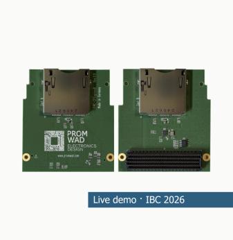
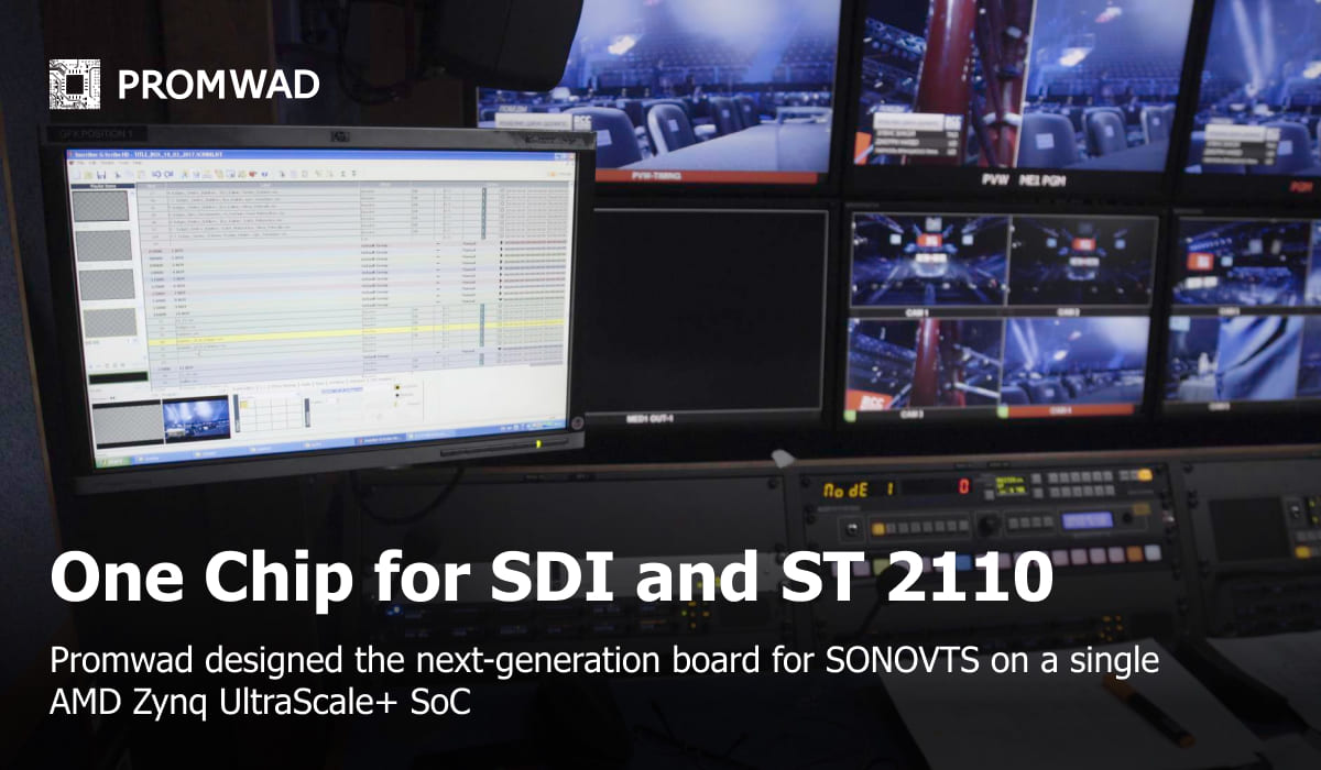
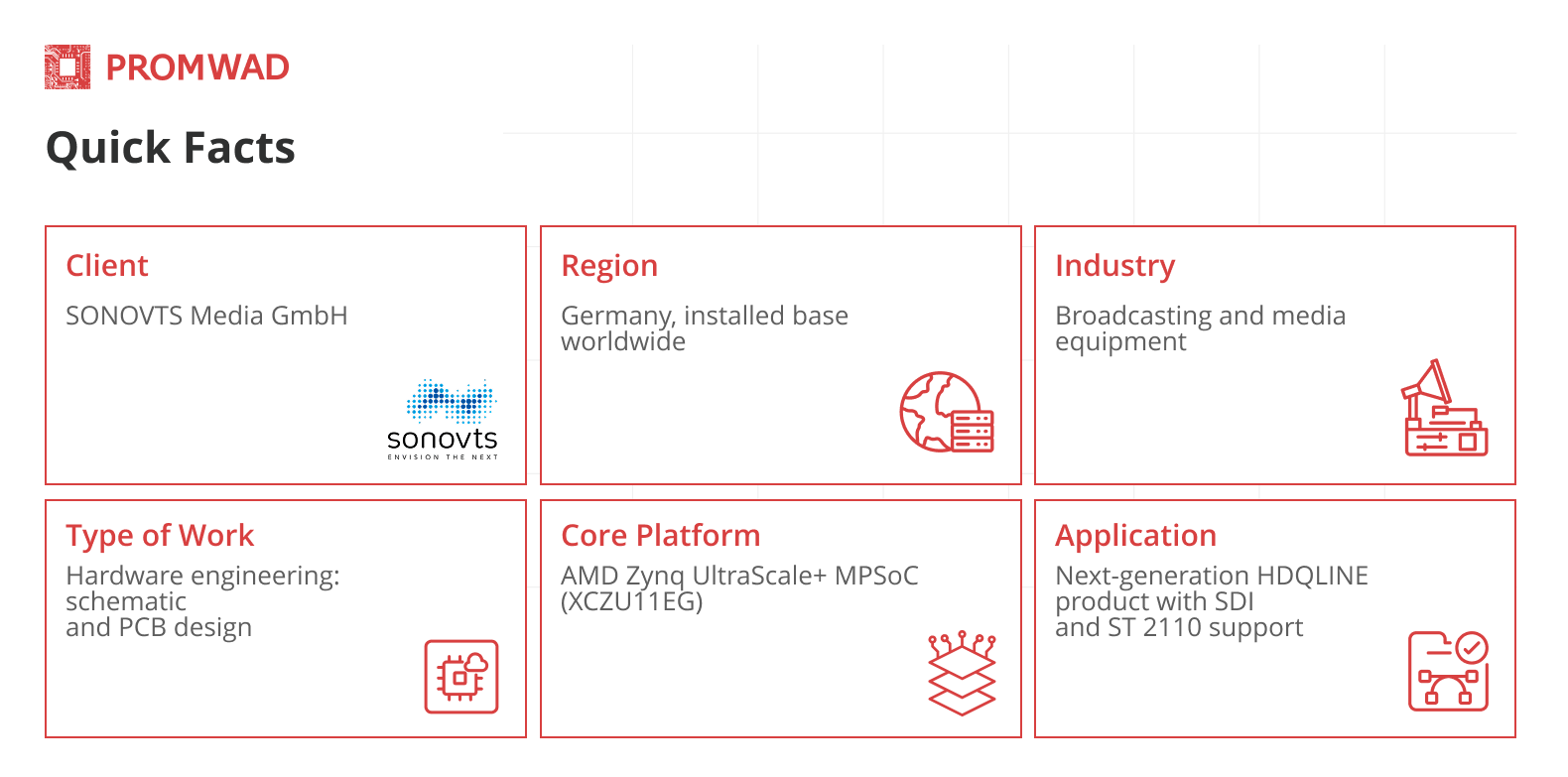
Project in a Nutshell: For SONOVTS Media GmbH, the company behind the HDQLINE professional broadcast display platform, Promwad designed the hardware platform for their next-generation product. The board is designed to handle both SDI and SMPTE ST 2110 IP signals on a single design, built on one AMD Zynq UltraScale+ chip in place of the two-chip architecture it replaces. It gives SONOVTS a hardware base prepared for the broadcast industry's move to IP.
Client & Challenge
SONOVTS Media GmbH is a German broadcast specialist behind HDQLINE, a professional UHD/4K broadcast display platform used in television studios, OB vans, and master control rooms worldwide.
SONOVTS has worked with IP-based broadcast standards for years, and their current HDQLINE generation already supports SMPTE ST 2110 through an optional I/O expansion module. The broadcast industry's shift to ST 2110 is now the procurement baseline for new master control rooms and production facilities. For the next product generation, ST 2110 support had to be part of the board's core hardware, not an optional add-on that raises the cost and integration effort of every unit.
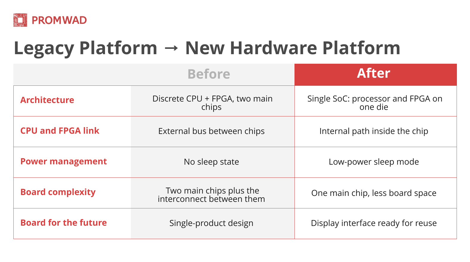
The client's previous board was built around a separate Texas Instruments Sitara processor and a Kintex UltraScale+ FPGA, and was no longer the right base for a product built around both SDI and ST 2110 from the core. Their engineering team focused on firmware and the display engine. They approached Promwad through an industry referral, looking for a hardware partner to redesign the platform around a modern SoC, while keeping FPGA firmware and board bring-up in-house.
Solution
We replaced the two-chip processing core with a single AMD Zynq UltraScale+ MPSoC, the XCZU11EG, where the application processor cluster and FPGA fabric sit on one die. This is the SoC class broadcast equipment manufacturers use for products that combine SDI capture with ST 2110 IP transport, because it places the video processing and the device's control functions on the same chip, which simplifies the design and reduces the component count.
The board brings the full input and output set onto one design:
- two 12G-SDI inputs through Semtech equalizers;
- HDMI and DisplayPort inputs supported by Parade and Texas Instruments retimers;
- Gigabit Ethernet for management;
- USB;
- LVDS and embedded DisplayPort outputs that drive the display panel.
The high-speed transceivers on the FPGA fabric carry the data path for the ST 2110 transport layer.
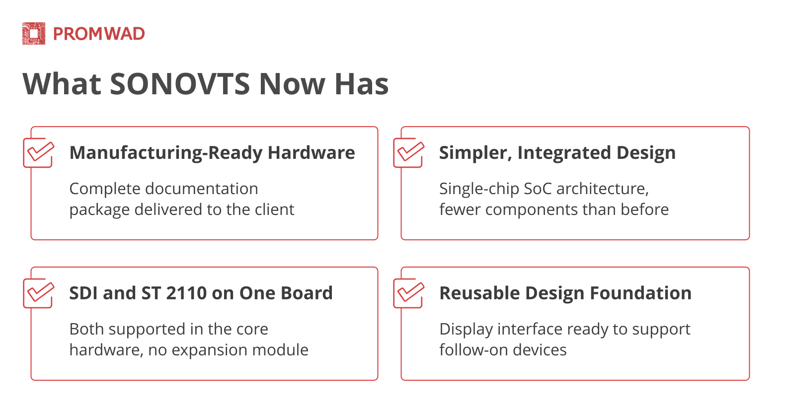
The power tree was redesigned from scratch around the new SoC, adding a low-power sleep state the previous board did not have. The display panel interface was structured to support reuse in follow-on devices in the HDQLINE family.
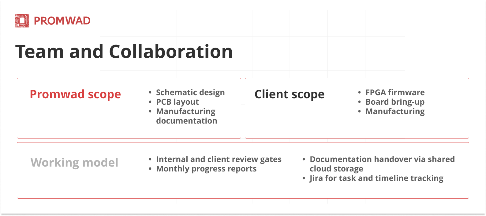
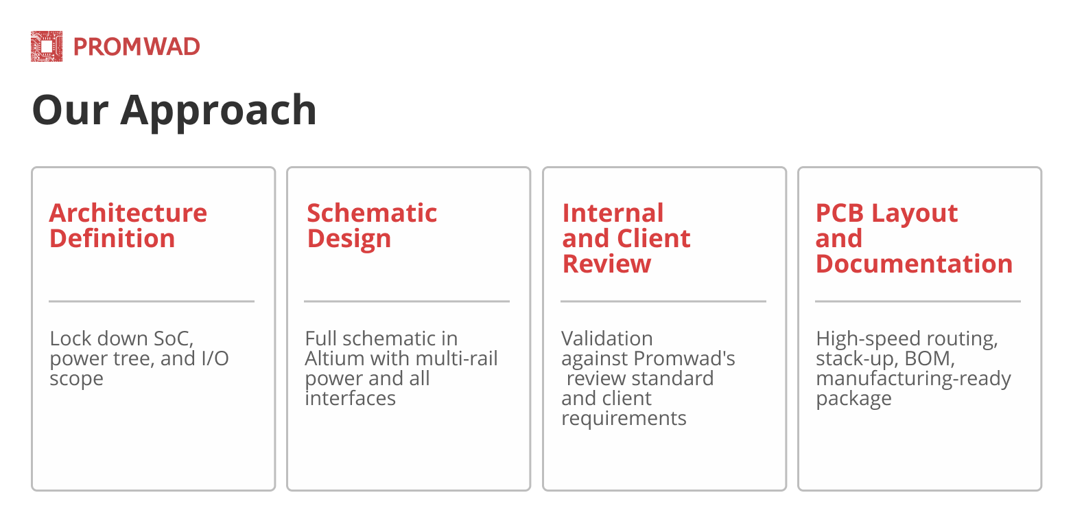
Hardware design was Promwad's scope on this project. The client's team owns manufacturing, board bring-up, and the FPGA firmware that runs on the platform.
Architecture and Key Decisions
The XCZU11EG was selected because it had the FPGA capacity and high-speed interfaces to handle 12G-SDI capture and ST 2110 packetization on one board, with room to spare for the full set of inputs and outputs. Consolidating two chips into one also freed board space the previous design spent on connecting them.
Results
Promwad delivered the hardware platform as a complete, manufacturing-ready documentation set. It gives SONOVTS the hardware base for the next generation of HDQLINE products, with SDI and ST 2110 support designed into the board itself.
Where Else This Works
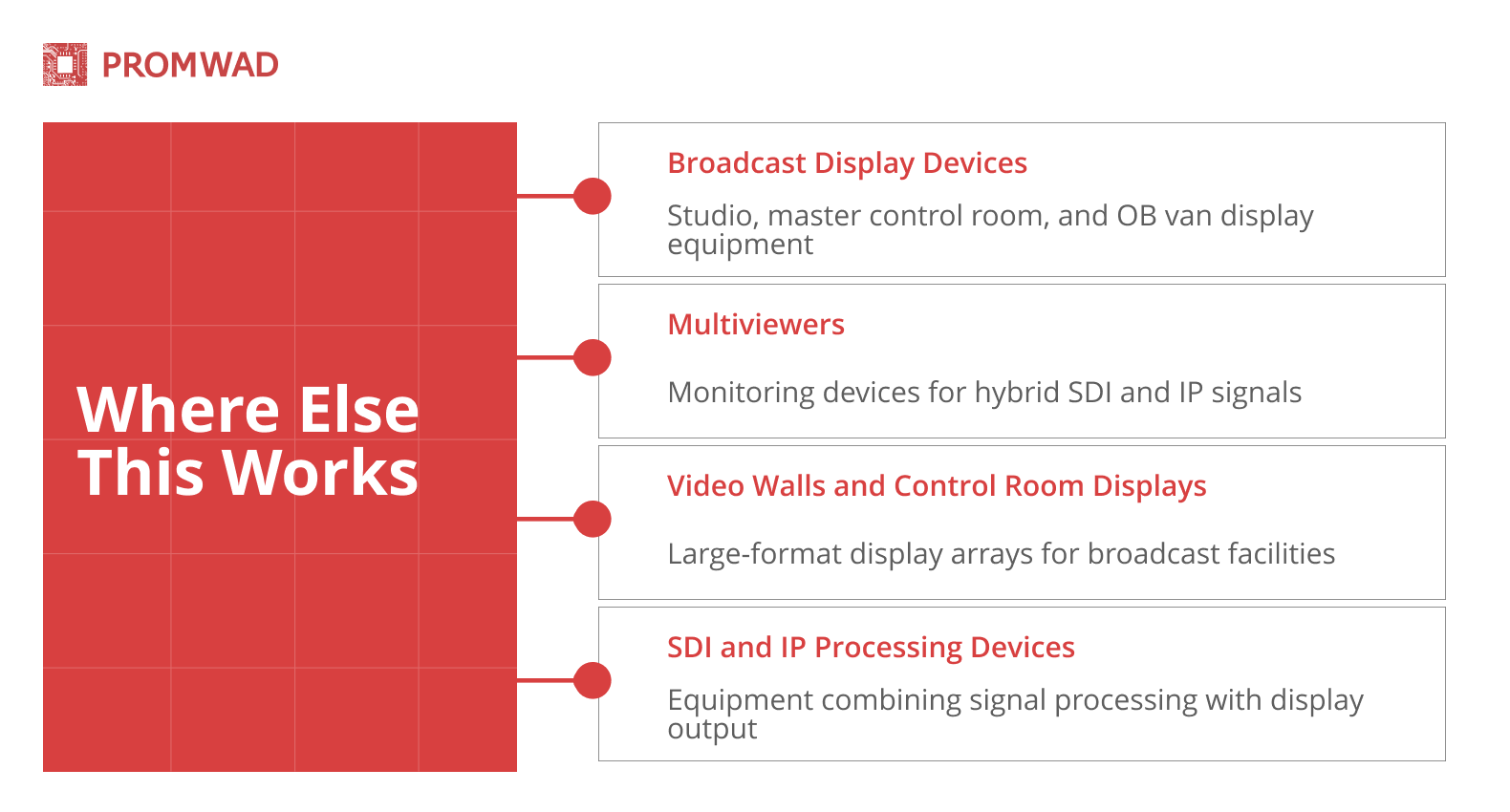
The same hardware base fits other broadcast devices that combine video capture with processing and display output: multiviewers, video walls, and IP-capable display and processing equipment.
More of What We Do for Broadcast Hardware
- ST 2110 Migration and NMOS Integration: how Promwad helps studios and OEMs move from SDI to SMPTE ST 2110 with predictable timing, NMOS discovery, and mixed-vendor interoperability.
- Enterprise Data Storage: an example of developing a scalable network storage solution with DPDK/SPDK support to improve data transfer speeds and network efficiency.
- NAB Show 2026: our take on the long road between SDI and ST 2110, and where hardware effort actually pays off for broadcast product companies.
FAQ
We're a broadcast equipment vendor moving toward hybrid SDI and ST 2110 designs. Can Promwad help if we only need the hardware layer?
Yes. Our broadcast engagements often start with a hardware-only scope: schematic and PCB for the next-generation device, while the client's team keeps FPGA firmware, bring-up, and manufacturing in-house. If your team is small and hardware is not where you invest internal capacity, that is the plug-in engineering model we are built for.
What broadcasting standards and FPGA platforms do you work with in your hardware projects?
In our broadcast equipment development projects, we work with the SMPTE ST 2110 standards (video, audio, auxiliary signals), PTP synchronization (IEEE 1588 / SMPTE ST 2059), AMWA NMOS control levels, the AES67 standard for audio, and IPMX for ProAV. As for platforms, our primary target platforms are the FPGA and SoC families from AMD, Altera, Lattice, and Microchip, and Promwad is a partner in these ecosystems.
Where should an SDI-to-ST 2110 migration start, and do we need to implement NMOS from day one?
A pragmatic starting point is an interop audit that identifies risks before large investments. From there: an architecture review (timing + network + control), readiness validation, a phased rollout plan, and a PoC/MVP that proves interoperability under realistic load. NMOS is not required on day one — many facilities migrate in phases: ST 2110 media transport first, with NMOS capabilities expanded gradually. The approach is aligned to your operational reality and risk tolerance.
Can Promwad join in "rescue mode" if a migration is already in trouble, and what does the team deliver?
Yes, the team plugs in at any stage (rescue, migration, or scaling) to stabilize the architecture, find root causes, build the missing validation, and get delivery back on a predictable track without restarting the project. The full stack is covered: FPGA logic (RTL / IP integration), embedded software, drivers, middleware, and control UI, plus verification assets such as latency and sync tests, regression hooks, and documentation for production readiness.
Do you build custom FPGA IP cores, or integrate commercial blocks, and how are they validated?
Both. Custom FPGA IP is developed for video (scaling, color space conversion, HDR paths, frame/line buffering with latency control, mixers, multiview, sync and timing alignment) and for audio (SRC/resampling, channel mapping, de-embed/embed, mixers, conditioning, high-density routing). Commercial IP is integrated when it accelerates time-to-market, including codec/processing blocks and AV-over-IP compliance components for ST 2110 / NMOS / AES67 / IPMX. Validation runs through interoperability matrices, regression tests, and system-level checks covering sync, lip-sync, and failure modes.