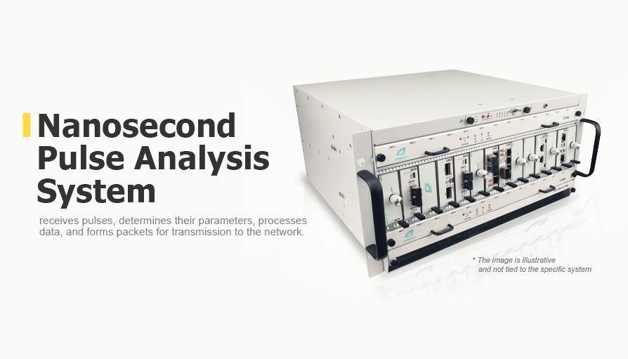
Software Development for Nanosecond Pulse Analysis System
Client
A German integrator of high-performance solutions.
Challenge
To develop and implement software for capturing and analysing nanosecond pulses.
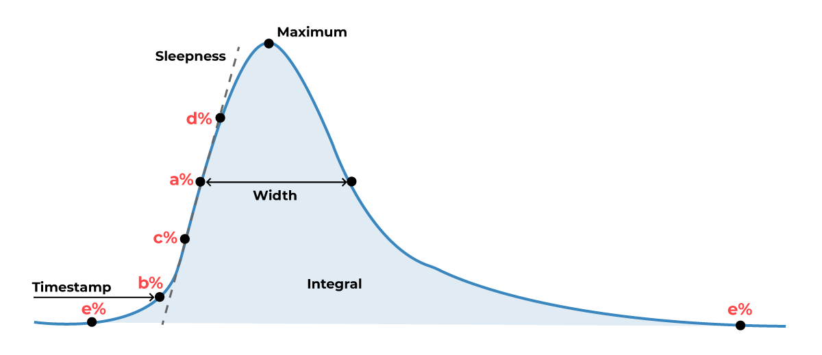
Figure 1. View of an impulse with the display of calculated parameters.
The main signal characteristics for testing are the pulse repetition rate of 10 kHz and the duration of 200 ns.
Solution
Hardware Design
We implemented the nanosecond pulse analysis system on the following MicroTCA platform:
- AMC599 x 6 pcs
- Xilinx UltraScale XCKU115 FPGA
- Quad ADC @ 3.2 GSPS with TI ADC12DJ3200
- UTC004, MicroTCA — Hub
- EM-AM4024 AMC — processor module
- 4th Gen Intel Core i7 Quad Core 1.8/2.4GHz
- 8/16 GB DDR3 ECC memory
Software Development
We implemented two functional parts: firmware and software for the system.
The firmware was developed on FPGA in the form of algorithms for detecting pulses, determining their parameters, filtering/processing and transferring data via the PCIe bus using DMA to the upper-level device. Compatibility between IP cores and modules was ensured using standard interfaces AXI4, AXI4-Lite, and AXI stream. We identified the functional parts of the system with the following design methods:
- Simulink + HDL coder
- Pulse detection.
- Impulse preprocessing (filtering).
- Emulation of system operation on debug boards and real experimental data.
- Event synchronisation module on different boards.
- HLS
- Calculation of parameters of nanosecond pulses.
- C++/Boost, x86 platform
- Statistics and data loading into DDR3 memory for testing.
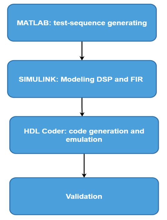
Figure 2. Firmware development algorithm
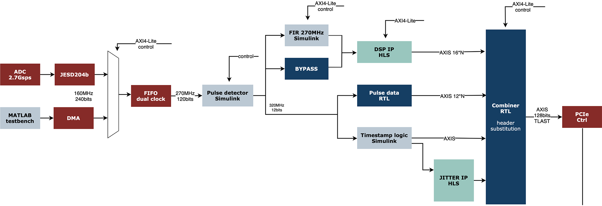
Figure 3. Functional diagram of the developed firmware
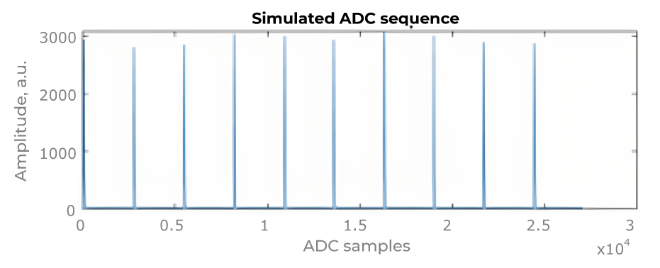
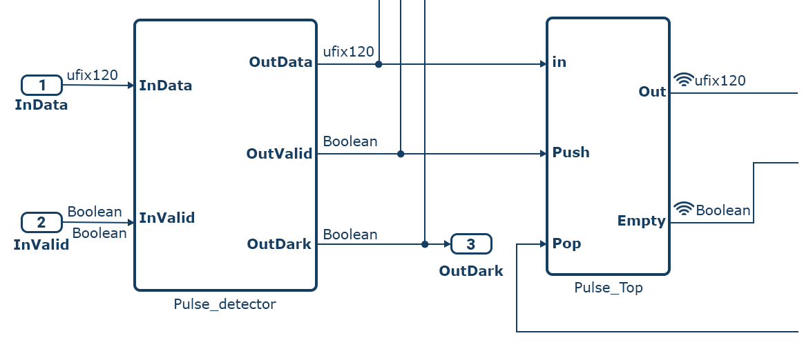
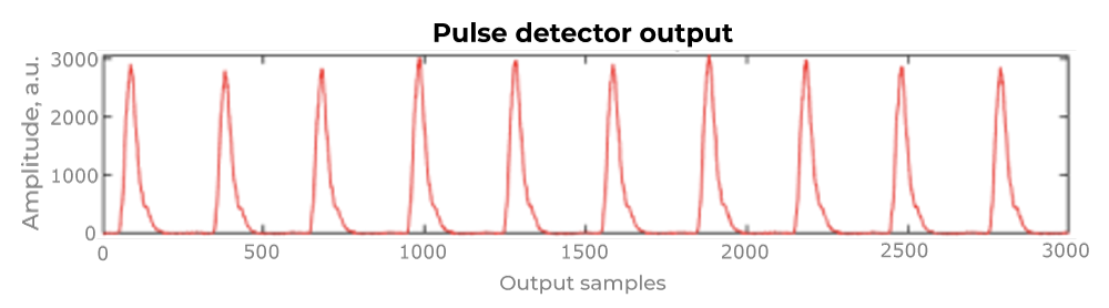
Figure 4. The simulation results in Simulink
Since the system is multichannel and physically separated, it is necessary to bind the detected pulses to time stamps. We developed an inter-board synchronisation module to do it.
Functions of the timestamp module (board-to-board synchronisation):
- synchronisation of boards;
- event registration;
- operating frequency — 156 MHz.
Our board-to-board synchronisation module interface:
- Inputs:
- Reset
- GPS sync: 1PPS
- Event
- Output:
- AXI stream with timestamps
The figure below shows the result of the module simulation in Simulink.
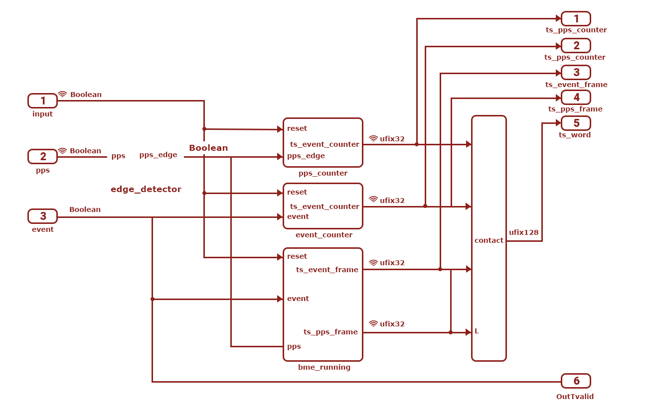
Figure 5. Model of the board-to-board synchronisation module
We implemented an algorithm for collecting/packing data via the PCIe bus, IP FW management functions through the control status registers (CSR) mechanism, resets and configuration features. Our software was also involved in forming TCP / IP packets for transmission to the network.
The figure below shows the diagram of the software part:
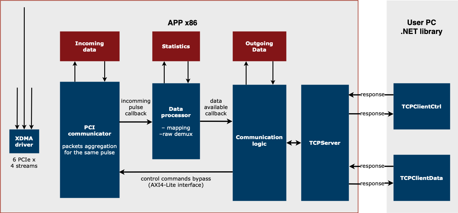
Figure 6. Scheme of the software part implementation
Business Value
As a result, we developed the software for our client's new nanosecond pulse analysis system that can receive pulses, determine their parameters, process data, and form packets with pulse parameters or the pulses themselves for transmission to the network.
Technologies we used within this project: PCIe; JESD 204b; Simulink; HLS; DMA; Linux; Microblaze; TCP/IP.
This is one of several projects that we have implemented with MTCA, an open standard for high-performance modular embedded systems. With MicroTCA, you get modularity, high scalability, and a compact design that reduces your time to market. Read more: How We Develop Custom AMC Boards and Integrate MicroTCA


