


Diffraction-based X-ray processing device design
Client
A world-leading security screening solutions provider.
Challenge
The client turned to Promwad to design a new X-ray-processing device. It is used to scan objects and determine their atomic structure. It quickly detects explosive materials.
Solution
1. Hardware Design
During the project, we designed the following printed circuit boards:
- Motherboard is the main carrier board. We installed FPGA SoM and measurement boards on it.
- Single Board is a measurement board with installed detectors and ASICs.
- Sync Board is an expansion card for the Motherboard; it builds up internal device synchronization.
The Motherboard is based on the Opal Kelly FPGA SoM XEM7310. That system-on-module is powered by our partner Xilinx's Artix-7 FPGA.
The Motherboard can monitor the following parameters:
- the board temperature and humidity;
- current consumption for each card rack;
- input supply voltage and current.
We installed a USB to three UART and one JTAG converter for the device debugging and diagnosis.
We installed six slots for enclosure fans to control the rotation speed for the cooling of the components.
The FPGA MachXO3 by our technology partner Lattice Semiconductor is installed to collect data from the ASICs and the higher boards and transfer the data to the lower board.
Another board component, the STM32L431 MCU by STMicroelectronics, is installed to update the firmware of the FPGA and upstream boards, control power and ASICs, and monitor the board temperature.
2. Software Development
The device contains many measurement boards that are identical in design and configuration. They don't differ from each other.
A MCU configures and controls the ASICs and other peripherals of its own measurement board: ADC, DAC, temperature sensor, power sensor. In addition, the MCU provides transport of control and monitoring commands from the Motherboard to the measurement boards.
The SPI interface transports commands and responses over a defined protocol. The main functional load is carried by the FPGA.
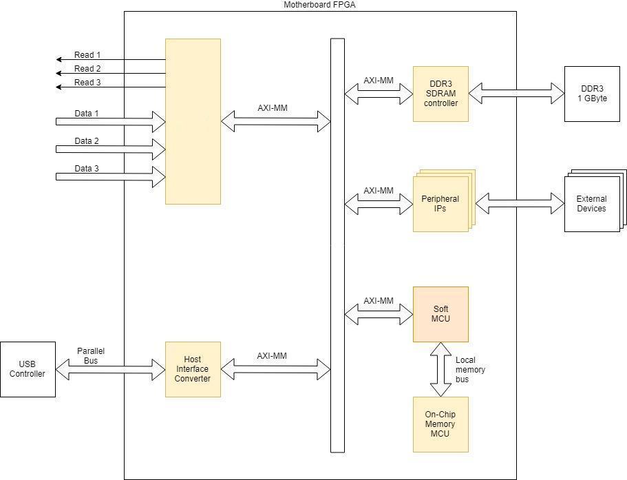
The Motherboard also contains an FPGA chip. Its main task is to collect data from all the measurement boards. At the core of the FPGA architecture is the AXI Memory Map system bus. All modules are connected to the AXI Memory Map, which provides flexibility and scalability of the system.
The main module on the bus is the microprocessor core Soft MCU, implemented on the logic resources of the FPGA. The MCU receives commands from the host via the USB bus and configures all other modules according to the given algorithm. The functional diagram is shown below.
3. Enclosure Mechanical Design
Within the project, we created industrial and mechanical design of an enclosure for an array of printed circuit boards with ASIC chips.
The main goal was to develop a device with minimal dimensions, compact board layout and cooling.
During the initial design phase, we performed thermal calculations to determine the optimal layout of components on the board, board-to-board clearances, enclosure design, and other characteristics.
We calculated nearly twenty iterations and chose the optimal one. During the computations, we changed the design of the back panel: it allowed us to redirect the flow through the board area.
The main enclosure parts are made of aluminum alloy and brass. The production method is milling. We also designed sheet plates with perforations at the fan mounting points. On the sensor side there is a 250-400 micron thick screen.
Business Value
We designed a sophisticated and unique industrial X-ray processing device with a number of competitive advantages for our customer:
- The energy resolution is very good, ~2Kev.
- Achieves higher photon registration event rate.
- Cheaper than competitors.
- Boards yield is at 97%.


